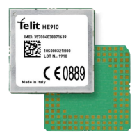
HE910 Hardware User Guide
1VV0300925 Rev. 32 Page 7 of 111 2019-11-25
11. USB HSIC .................................................................................. 75
12. SERIAL PORTS ......................................................................... 77
MODEM SERIAL PORT 1 (USIF0) ............................................. 78
MODEM SERIAL PORT 2 (USIF1) ............................................. 81
RS232 level translation ............................................................... 82
13. AUDIO SECTION OVERVIEW ................................................... 84
Electrical Characteristics ............................................................. 84
13.1.1. CODEC Examples ...................................................................... 84
14. GENERAL PURPOSE I/O .......................................................... 85
GPIO Logic levels ....................................................................... 86
Using a GPIO Pad as INPUT ...................................................... 87
Using a GPIO Pad as OUTPUT .................................................. 87
Indication of network service availability ..................................... 88
RTC Bypass out .......................................................................... 89
External SIM Holder Implementation ........................................... 89
VAUX Power Output ................................................................... 89
ADC Converter ........................................................................... 90
14.8.1. Description .................................................................................. 90
14.8.2. Using ADC Converter ................................................................. 90
15. MOUNTING THE HE910 ON THE APPLICATION ..................... 91
General ....................................................................................... 91
Module finishing & dimensions .................................................... 91
Recommended foot print for the application ................................ 93
Stencil ......................................................................................... 94
PCB pad design .......................................................................... 94
PCB pad dimensions .................................................................. 95
Solder paste ............................................................................... 97
15.7.1. HE910 Solder reflow ................................................................... 97
Packing system (Tray) ................................................................ 99
Packing System (Reel) ............................................................. 102
15.9.1. Carrier Tape Detail ................................................................... 102
15.9.2. Reel Detail ................................................................................ 103
15.9.3. Packaging Detail ....................................................................... 104
Moisture sensitivity ................................................................... 104
16. SAFETY RECOMMANDATIONS ............................................. 105
FCC/IC Regulatory notices ....................................................... 106