Enable by pulling PWDNB low
Input clock is gated by PWDNB, no SCCB
communication
Register value are maintained
Power down all blocks and regulator
Low power consumption
GPIO can be configured as high/low/tri-state
◼ Design Tools
⚫ Quartus II v15.0
⚫ Nios II Eclipse 15.0
◼ Demonstration Source Code
⚫ Quartus project directory: DE1_SOC_D8MX2_VIP
⚫ Nios II Eclipse project workspace: DE1_SOC_D8M_VIP\software
◼ Demonstration Batch File
⚫ Demo batch file folder: demonstrations\DE1_SOC_D8MX2_VIP\demo_batch
◼ Demonstration Setup
⚫ Connect a USB cable between the host PC and the USB connector (J13) on
the DE1-SOC board.
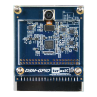
⚫ Connect the two D8M modules to GPIO0 (JP1) and GPIO1 (JP2) on
DE1-SOC board (See Figure 5-5).
⚫ Connect the VGA output of the DE1-SOC board to a VGA monitor.


 To Next Page