Resource
nRSTOUT TPS65941213-Q1
PMIC Delay Diagram Total Delay Rail Name
0 us H_MCU_PORz_1V8
nRSTOUT_SOC TPS65941213-Q1 0 us H_SOC_PORz_1V8
BUCK3 Monitor TPS65941213-Q1 0 us mVDD_MCUIO_3V3
LDO3 TPS65941213-Q1 0 us VDD_DLL_0V8
BUCK123 TPS65941213-Q1 0 us VDD_CPU(AVS)
BUCK4 TPS65941213-Q1 0 us VDD_MCU_0V85
BUCK5 TPS65941213-Q1 0 us VDD_PHY_1V8
LDO2 TPS65941213-Q1 0 us VDD_MCUIO_1V8
LDO4 TPS65941213-Q1 0 us VDA_MCU_1V8
LDO1 TPS65941213-Q1 0 us VDD1_DDR_1V8
GPIO9 TPS65941213-Q1 0 us EN_MCU3V3IO_LDSW
GPIO3 TPS65941111-Q1 0 us EN_VDDR
BUCK5 TPS65941111-Q1 0 us VDD_RAM_0V85
LDO3 TPS65941111-Q1 0 us VDD_IO_1V8
BUCK1234 TPS65941111-Q1 0 us VDD_CORE_0V8
LDO4 TPS65941111-Q1 0 us VDA_PLL_1V8
LDO1 TPS65941111-Q1
0 us VDD_SD_DV
LDO2 TPS65941111-Q1 0 us VDD_USB_3V3
GPIO11 TPS65941111-Q1 0 us EN_3V3IO_LDSW
EN_DRV TPS65941213-Q1 0 us EN_DRV
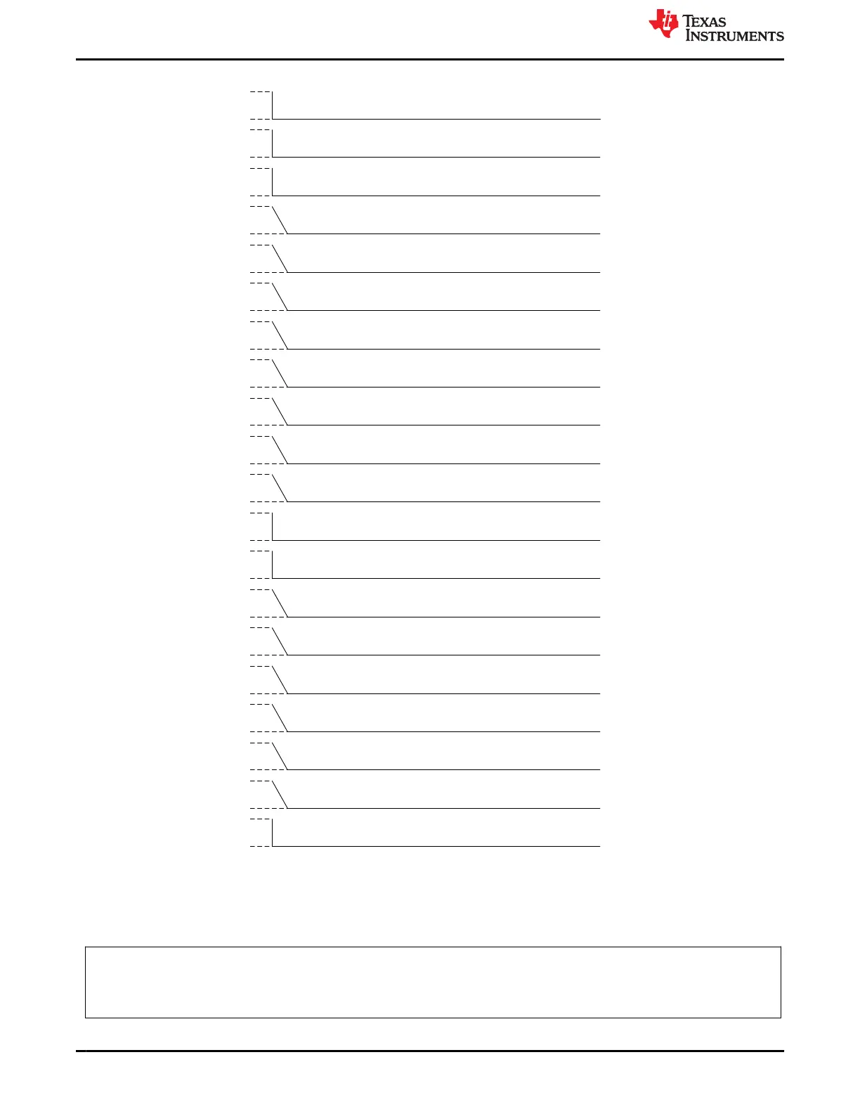
Figure 6-2. TO_SAFE_SEVERE and TO_SAFE Power Sequences
After the power sequence shown in Figure 6-2, the TO_SAFE sequence delays the TPS65941213 by 16 ms and
the TPS65941111 by 3 ms. This ensures that the primary PMIC finishes after the secondary. After these delays,
the following instructions are executed on both PMICs:
//TPS65941213 and TPS65941111
// Clear AMUXOUT_EN, CLKMON_EN, set LPM_EN
REG_WRITE_MASK_IMM ADDR=0x81 DATA=0x04 MASK=0xE3
// Reset all BUCK regulators
REG_WRITE_MASK_IMM ADDR=0x87 DATA=0x1F MASK=0xE0
Pre-Configurable Finite State Machine (PFSM) Settings www.ti.com
36 Optimized Dual TPS6594-Q1 PMIC User Guide for Jacinto
™
7 DRA829 or
TDA4VM Automotive PDN-0C
SLVUC99 – JANUARY 2022
Submit Document Feedback
Copyright © 2022 Texas Instruments Incorporated
 Loading...