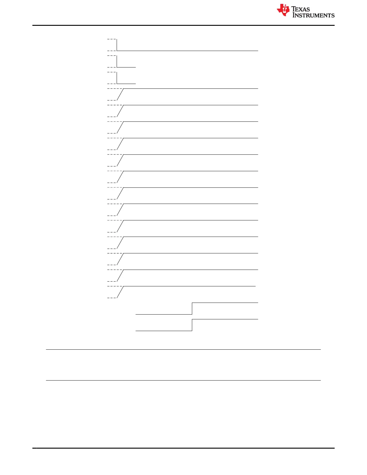
Resource
nRSTOUT TPS65941213-Q1
PMIC Delay Diagram Total Delay Rail Name
0 us H_MCU_PORz_1V8
nRSTOUT_SOC TPS65941213-Q1 0 us H_SOC_PORz_1V8
LDO3 TPS65941213-Q1 0 us VDD_DLL_0V8
BUCK123 TPS65941213-Q1 0 us VDD_CPU(AVS)
BUCK4 TPS65941213-Q1 0 us VDD_MCU_0V85
BUCK5 TPS65941213-Q1 0 us VDD_PHY_1V8
LDO2 TPS65941213-Q1 0 us VDD_MCUIO_1V8
LDO4 TPS65941213-Q1 0 us VDA_MCU_1V8
LDO1 TPS65941213-Q1 0 us VDD1_DDR_1V8
BUCK5 TPS65941111-Q1
0 us VDD_RAM_0V85
LDO3 TPS65941111-Q1
0 us VDD_IO_1V8
BUCK1234 TPS65941111-Q1 0 us VDD_CORE_0V8
LDO4 TPS65941111-Q1 0 us VDA_PLL_1V8
LDO1 TPS65941111-Q1 0 us VDD_SD_DV
LDO2 TPS65941111-Q1 0 us VDD_USB_3V3
nRSTOUT TPS65941213-Q1
2000 us H_MCU_PORz_1V8
nRSTOUT_SOC TPS65941213-Q1 2000 us H_SOC_PORz_1V8
EN_DRV TPS65941213-Q1 0 us EN_DRV
Figure 6-4. ACTIVE_TO_WARM Power Sequence
Note
The regulator transitions do not represent enabling of the regulators but the time at which the voltages
are restored to their default values. Since this sequence originates from the ACTIVE state all of the
regulators are on.
6.3.4 ESM_SOC_ERROR
In the event of an ESM_SOC error, the nRSTOUT_SOC signal is driven low and then driven high again after 200
µs. There is no change to the power rails. The sequence is shown in Figure 6-5.
Pre-Configurable Finite State Machine (PFSM) Settings www.ti.com
40 Optimized Dual TPS6594-Q1 PMIC User Guide for Jacinto
™
7 DRA829 or
TDA4VM Automotive PDN-0C
SLVUC99 – JANUARY 2022
Submit Document Feedback
Copyright © 2022 Texas Instruments Incorporated
 Loading...