Appendix A Differences Between Devices and BSL Versions
Appendix A
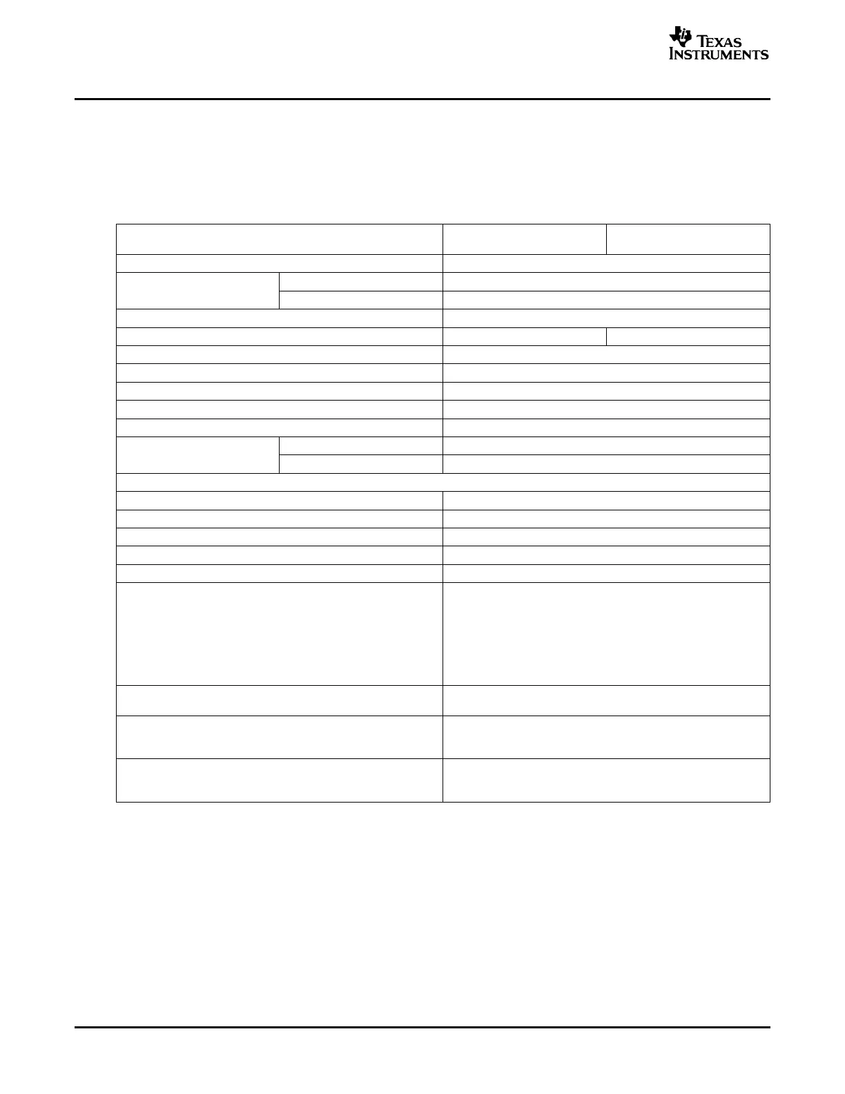
In summary, the tables in this appendix show the key information of MSP430 device/BSL version
assignment related to their hard/software resources.
Table A-1. BSL Version 1.10 on F13x, F14x(1), F11x, and F11x1
F13x F11x (obsolete)
Device
F14x(1) F11x1 (obsolete)
BSL Version 1.10
Cold start 0C00h
BSL vector address
Warm start —
Chip ID address 0FF0h
Chip ID data F149h F112h
BSL version address 0FFAh
BSL version data 0110h
Mass erase time, nominal (ms) 17.2
(1)
Read/write access at 0000h–FFFFh Byte
Verification during write (online) No
SP critical 021Ah
Stack pointer initialization
SP not critical Unchanged
Resources Used by BSL
Transmit pin (TX)/Receive pin (RX) P 1.1 / P2.2
RAM/stack used 0200h–0219h
Working registers R5–R9
System clock, affected controls BCSCTL1, DCOCTL
Timer_A, affected controls TACTL, TAR, CCTL0, CCR0
mov #00h, &CCTL0
bic.b #02h, &P1SEL
bic.b #04h, &P2SEL
Preparation for SW call
bic.b #32h, &IE1
mov.b #00h, &BCSCTL2
mov #00h, SR
br &0C00h
Comment 1 Load PATCH.TXT to eliminate ROM bug. See chapters ”Special
Workaround mandatory: Considerations for BSL Version 1.10” and “Loadable BSL”.
Comment 2 Load BL_150S_14x.txt to get all features of V1.60 plus valid
Optional for F148, F149 only: Use loadable BSL erase segment command: See chapter “Loadable BSL”.
(>1KB RAM required)
Comment 3 Load BS_150S_14x.txt to get some features of V1.60: See
Optional for F1x4 … F1x9: Use small loadable BSL chapter “Loadable BSL”.
(<512B RAM required)
(1)
To reach the required mass erase time as specified in the datasheet the mass erase command has to be executed several
times.
16 Features of the MSP430 Bootstrap Loader SLAA089D – December 1999 – Revised August 2006
Submit Documentation Feedback