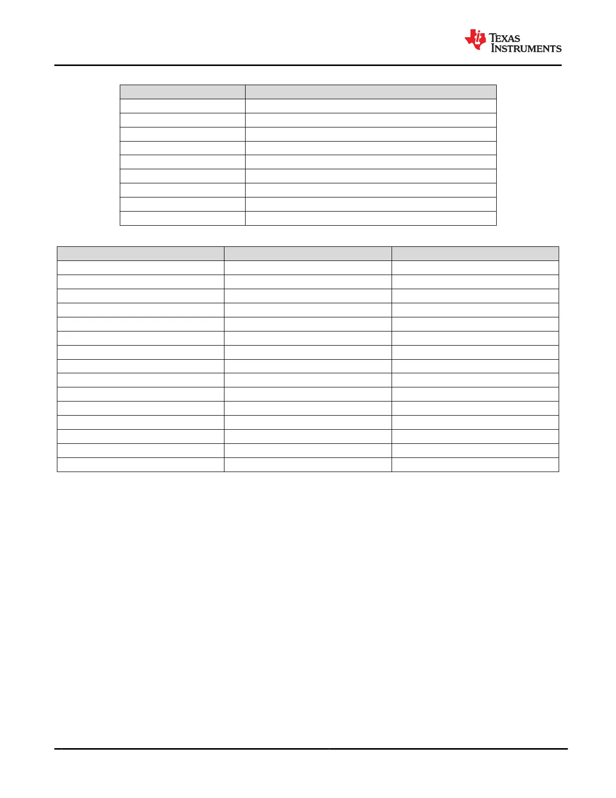
Table 9-7. I/O Buffer Type Description
BUFFER TYPE DESCRIPTION
IOBUF_GPIOHSSWD General Purpose High-Speed I/O
IOBUF_GPIOHSSPI General Purpose High-Speed I/O
IOBUF_GPIOLS General Purpose Low-Speed I/O
IOBUF_GPIOLSI2C General Purpose Low-Speed I/O with I
2
C deglitch time
IOBUF_I2C I
2
C Compliant Clock/Data Buffers
IOBUF_OD Open-Drain Output
IOBUF_UTX Push-Pull output buffer for UART
IOBUF_URX Input buffer for UART
IOBUF_PORT Input buffer between 1st/2nd stage Port Data Mux
Table 9-8. Pin to I/O Buffer Mapping
I/O GROUP/PIN BUFFER TYPE SUPPLY CONNECTION (DEFAULT FIRST)
DEBUG1/2/3/4 IOBUF_GPIOLS LDO_3V3, VDDIO
DEBUG_CTL1/2 IOBUF_GPIOLSI2C LDO_3V3, VDDIO
BUSPOWERZ IOBUF_GPIOLS LDO_3V3, VDDIO
GPIO0-8 IOBUF_GPIOLS LDO_3V3, VDDIO
I2C_IRQ1/2Z IOBUF_OD LDO_3V3, VDDIO
I2C_SDA1/2/SCL/1/2 IOBUF_I2C LDO_3V3, VDDIO
LSX_P2R IOBUF_UTX LDO_3V3, VDDIO
LSX_R2P IOBUF_URX LDO_3V3, VDDIO
MRESET IOBUF_GPIOLS LDO_3V3, VDDIO
RESETZ IOBUF_GPIOLS LDO_3V3, VDDIO
UART_RX IOBUF_URX LDO_3V3, VDDIO
UART_TX IOBUF_UTX LDO_3V3, VDDIO
PORT_INT IOBUF_PORT LDO_3V3
SPI_PICO/POCI/CLK/CSZ IOBUF_GPIOHSSPI LDO_3V3
SWD_CLK/DATA IOBUF_GPIOHSSWD LDO_3V3
9.3.18.1 IOBUF_GPIOLS and IOBUF_GPIOLSI2C
Figure 9-45 shows the GPIO I/O buffer for all GPIOn pins listed GPIO0-GPIO17 in Pin Configuration and
Functions. GPIOn pins can be mapped to USB Type-C, USB PD, and application-specific events to control
other ICs, interrupt a host processor, or receive input from another IC. This buffer is configurable to be a
push-pull output, a weak push-pull, or open drain output. When configured as an input, the signal can be a
deglitched digital input or an analog input to the ADC. The push-pull output is a simple CMOS output with
independent pulldown control allowing open-drain connections. The weak push-pull is also a CMOS output,
but with GPIO_RPU resistance in series with the drain. The supply voltage to this buffer is configurable to be
LDO_3V3 by default or VDDIO. For simplicity, the connection to VDDIO is not shown in Figure 9-45, but the
connection to VDDIO is fail-safe and a diode will not be present from GPIOn to VDDIO in this configuration. The
pullup and pulldown output drivers are independently controlled from the input and are enabled or disabled via
application code in the digital core.
TPS65982
SLVSD02E – MARCH 2015 – REVISED AUGUST 2021
www.ti.com
66 Submit Document Feedback
Copyright © 2021 Texas Instruments Incorporated
Product Folder Links: TPS65982