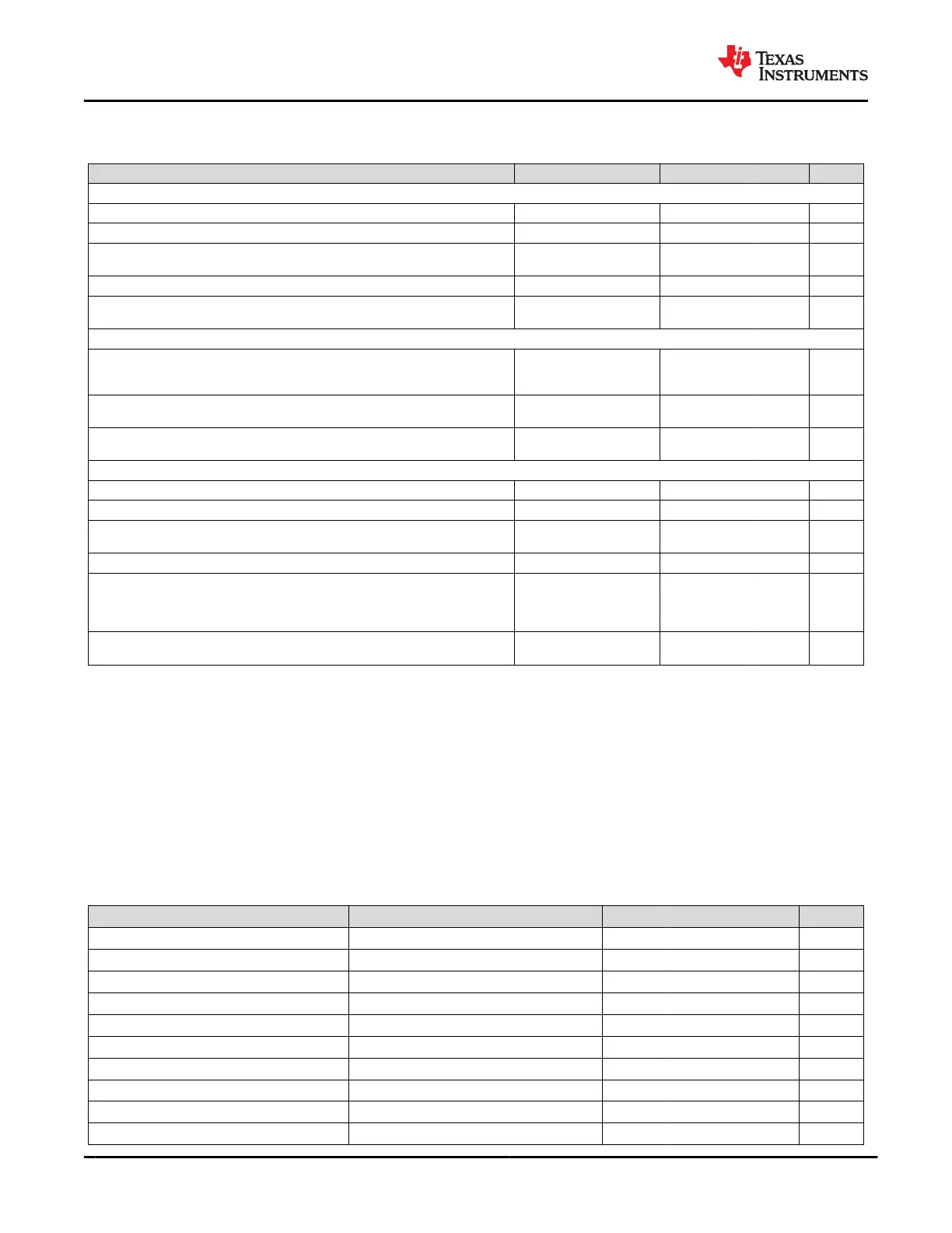
7.9 USB-PD Baseband Signal Requirements and Characteristics
Recommended operating conditions; T
A
= –10 to 85°C unless otherwise noted
PARAMETER TEST CONDITIONS MIN TYP MAX UNIT
COMMON
PD_BITRATE PD data bit rate 270 300 330 Kbps
UI
(1)
Unit interval (1/PD_BITRATE) 3.03 3.33 3.7 μs
CCBLPLUG
(2)
Capacitance for a cable plug (each plug on a cable may have up
to this value)
25 pF
ZCABLE Cable characteristic impedance 32 65 Ω
CRECEIVER
(3)
Receiver capacitance. Capacitance looking into C_CCn pin when
in receiver mode
70 120 pF
TRANSMITTER
ZDRIVER
TX output impedance. Source output impedance at the Nyquist
frequency of USB2.0 low speed (750kHz) while the source is
driving the C_CCn line
33 75 Ω
TRISE
Rise Time. 10% to 90% amplitude points, minimum is under an
unloaded condition. Maximum set by TX mask
300 ns
TFALL
Fall Time. 90% to 10% amplitude points, minimum is under an
unloaded condition. Maximum set by TX mask
300 ns
RECEIVER
VRXTR Rx Receive Rising Input threshold 605 630 655 mV
VRXTF Rx Receive Falling Input threshold 450 470 490 mV
NCOUNT
(4)
Number of transitions for signal detection (number to count to
detect non-idle bus)
3
TTRANWIN
(4)
Time window for detecting non-idle bus 12 20 μs
ZBMCRX Receiver input impedance
Does not include pullup or
pulldown resistance from
cable detect. Transmitter is
Hi-Z.
10 MΩ
TRXFILTER
(5)
Rx bandwidth limiting filter. Time constant of a single pole filter to
limit broadband noise ingression
100 ns
(1) UI denotes the time to transmit an un-encoded data bit not the shortest high or low times on the wire after encoding with BMC. A single
data bit cell has duration of 1 UI, but a data bit cell with value 1 will contain a centrally place 01 or 10 transition in addition to the
transition at the start of the cell.
(2) The capacitance of the bulk cable is not included in the CCBLPLUG definition. It is modeled as a transmission line.
(3) CRECEIVER includes only the internal capacitance on a C_CCn pin when the pin is configured to be receiving BMC data. External
capacitance is needed to meet the required minimum capacitance per the USB-PD Specifications. TI recommends to add capacitance
to bring the total pin capacitance to 300 pF for improved TX behavior.
(4) BMC packet collision is avoided by the detection of signal transitions at the receiver. Detection is active when a minimum of NCOUNT
transitions occur at the receiver within a time window of TTRANWIN. After waiting TTRANWIN without detecting NCOUNT transitions,
the bus is declared idle.
(5) Broadband noise ingression is because of coupling in the cable interconnect.
7.10 USB-PD TX Driver Voltage Adjustment Parameter
Recommended operating conditions; T
A
= –10 to 85°C unless otherwise noted
(1)
PARAMETER TEST CONDITIONS MIN NOM MAX UNIT
VTXP0 TX transmit peak voltage 1.615 1.7 1.785 V
VTXP1 TX transmit peak voltage 1.52 1.6 1.68 V
VTXP2 TX transmit peak voltage 1.425 1.5 1.575 V
VTXP3 TX transmit peak voltage 1.33 1.4 1.47 V
VTXP4 TX transmit peak voltage 1.235 1.3 1.365 V
VTXP5 TX transmit peak voltage 1.188 1.25 1.312 V
VTXP6 TX transmit peak voltage 1.14 1.2 1.26 V
VTXP7 TX transmit peak voltage 1.116 1.175 1.233 V
VTXP8 TX transmit peak voltage 1.092 1.15 1.208 V
VTXP9 TX transmit peak voltage 1.068 1.125 1.181 V
TPS65982
SLVSD02E – MARCH 2015 – REVISED AUGUST 2021
www.ti.com
16 Submit Document Feedback
Copyright © 2021 Texas Instruments Incorporated
Product Folder Links: TPS65982