Cinterion
®
LGA DevKit User Guide
Contents
36
t lga_devkit_ug_v03 2020-05-29
Public / Released
Page 3 of 36
Contents
1 Introduction ................................................................................................................. 5
1.1 Feature and Benefits.......................................................................................... 5
1.2 Supported Products ........................................................................................... 6
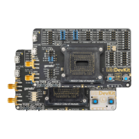
1.3 Package Content ............................................................................................... 7
2 Quickstart .................................................................................................................... 9
2.1 Mounting the LGA DevKit Socket ...................................................................... 9
3 LGA DevKit Overview ............................................................................................... 10
3.1 Top and Underside View.................................................................................. 10
3.2 Block Diagram.................................................................................................. 11
4 LGA DevKit Interfaces .............................................................................................. 12
4.1 USB.................................................................................................................. 12
4.2 SIM................................................................................................................... 12
4.3 Pin Headers ..................................................................................................... 13
4.3.1 Default Configuration .......................................................................... 13
4.4 ON Button: Module Start and Power Down ..................................................... 14
4.5 RST Button: Module Reset .............................................................................. 14
4.6 ASC0 Switch: Module UART Interface Selection............................................. 14
4.7 PWR Switch: Power Source Selection............................................................. 14
4.8 Free Level Shifters........................................................................................... 15
4.9 LEDs ................................................................................................................ 15
4.10 Patch Field ....................................................................................................... 15
4.11 RF Antenna...................................................................................................... 16
4.12 Power Supply................................................................................................... 17
4.12.1 Supply Current Measurement ............................................................. 17
4.12.2 External Reference Supply ................................................................. 18
5 General Characteristics............................................................................................ 19
6 Operating the LGA DevKit with a DSB .................................................................... 20
6.1 LGA DevKit on DSB-Mini ................................................................................. 20
6.2 LGA DevKit on DSB75..................................................................................... 21
7 Module Specific Configuration Settings ................................................................. 22
7.1 BGS1 and BGS2 Operation ............................................................................. 22
7.2 BGS12 Operation............................................................................................. 22
7.3 EMS31 Operation ............................................................................................ 22
7.4 ENS22 Operation............................................................................................. 23