6
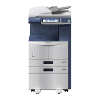
© 2007 - 2008 TOSHIBA TEC CORPORATION All rights reserved e-STUDIO167/207/237
SCANNER
6 - 9
6.5.2 CCD control circuit
On the contact image sensor (CIS) unit, CCD (Charge Coupled Device) with 7,084 effective pixels are
mounted as the optoelectronic element for converting the light reflected on the original into electrical
signals (analog signals). CCD is driven by the clock signals (TRCLCK, MCLCK, RSCLCK) output from
the SoC on the MAIN board, and then it divides the photoelectric-converted analog signals into four out-
put signals (CDIN0 to 3) and outputs to the AFE. The AFE converts the analog signals into 8-bit digital
signals (SCNIMGA [0] to [7]) and outputs to the SoC.
Fig. 6-5
SoC
AFE
CCD
MAIN board Contact image sensor unit
+5V
SH TRCLCK
CK2B MCLCK
RS RSCLCK
CDIN1
CDIN2
CDIN3
CDIN4
SCNIMGA[0]
SCNIMGA[1]
SCNIMGA[2]
SCNIMGA[3]
SCNIMGA[4]
SCNIMGA[5]
SCNIMGA[6]
SCNIMGA[7]
IMGDTA[0]
IMGDTA[1]
IMGDTA[2]
IMGDTA[3]
IMGDTA[4]
IMGDTA[5]
IMGDTA[6]
IMGDTA[7]
 Loading...