SARA-G450 - System integration manual
UBX-18046432 - R08 Design-in Page 112 of 143
C1-Public
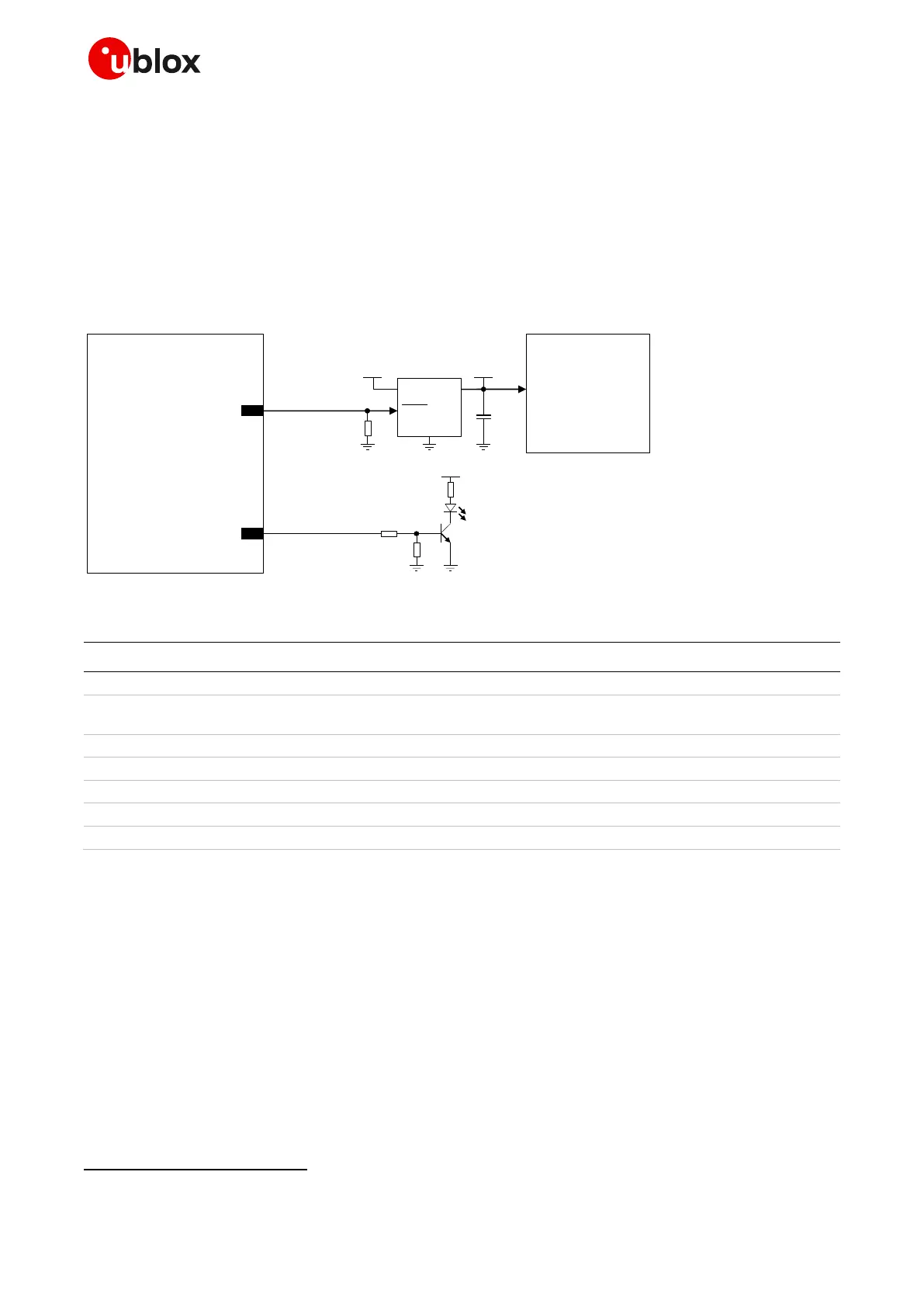
2.8 General Purpose Input/Output (GPIO)
2.8.1.1 Guidelines for GPIO circuit design
The following application circuit is suggested as a general guideline for the usage of the GPIO pins
available with the SARA-G450 modules, according to the related custom function.
Figure 71 describes an application circuit for a typical usage of some GPIO functions of the modules:
“Network indication” function provided by the GPIO1 pin
“GNSS supply enable” function provided by the GPIO2 pin
OUTIN
GND
LDO regulator
SHDN
3V8 1V8
R1
VCC
GPIO2 23
SARA-G450
u-blox GNSS
1.8 V receiver
U1
C1
R2
R4
3V8
Network indication
R3
GNSS supply enable
16
GPIO1
DL1
T1
Figure 71: GPIO application circuit
Part number - Manufacturer
47 kΩ resistor 0402 5% 0.1 W
Voltage regulator for GNSS receiver and related
output bypass capacitor
See GNSS module hardware integration manual
10 kΩ resistor 0402 5% 0.1 W
47 kΩ resistor 0402 5% 0.1 W
820 Ω resistor 0402 5% 0.1 W
LTST-C190KRKT - Lite-on Technology Corporation
Table 45: Components for GPIO application circuit
☞ Use transistors with at least an integrated resistor in the base pin or otherwise put a 10 kΩ resistor
on the board in series to the GPIO.
☞ The ESD sensitivity rating of the GPIO pins is 1 kV (Human Body Model according to JESD22-A114).
A higher protection level could be required if the lines are externally accessible on the application
board. This higher protection level can be achieved by mounting an ESD protection (e.g. EPCOS
CA05P4S14THSG varistor array) close to accessible points.
Not supported by the “00” product version
 Loading...