SARA-R5 series - System integration manual
UBX-19041356 - R04 Design-in Page 57 of 118
C1-Public
If the distance between the transmission line and the adjacent GND area (on the same layer) does not
exceed 5 times the width of the line, use the “Coplanar Waveguide” model for the 50 calculation.
Additionally to the 50 impedance, the following guidelines are recommended for transmission lines:
• Minimize the transmission line length: the insertion loss should be minimized as much as possible,
in the order of a few tenths of a dB,
• Add GND keep-out (i.e. clearance, a void area) on buried metal layers below any pad of component
present on the RF transmission lines, if top-layer to buried layer dielectric thickness is below
200 m, to reduce parasitic capacitance to ground,
• The transmission lines width and spacing to GND must be uniform and routed as smoothly as
possible: avoid abrupt changes of width and spacing to GND,
• Add GND stitching vias around transmission lines, as described in Figure 35,
• Ensure solid metal connection of the adjacent metal layer on the PCB stack-up to main ground
layer, providing enough vias on the adjacent metal layer, as described in Figure 35,
• Route RF transmission lines far from any noise source (as switching supplies and digital lines) and
from any sensitive circuit (as USB),
• Avoid stubs on the transmission lines,
• Avoid signal routing in parallel to transmission lines or crossing the transmission lines on buried
metal layer,
• Do not route microstrip lines below discrete component or other mechanics placed on top layer
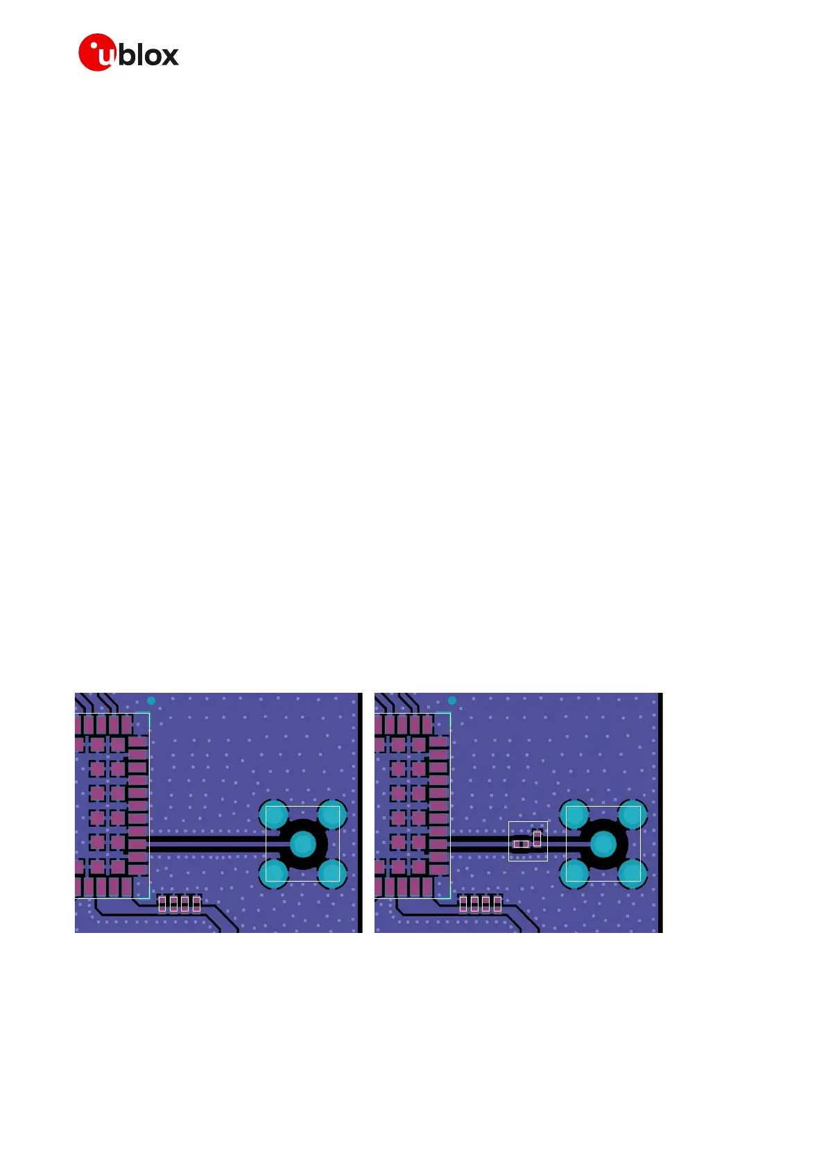
Two examples of a suitable RF circuit design for ANT pin are illustrated in Figure 35, where the cellular
antenna detection circuit is not implemented (if the cellular antenna detection function is required by
the application, follow the guidelines for circuit and layout implementation detailed in section 2.4.5):
• In the first example shown on the left, the ANT pin is directly connected to an SMA connector by
means of a suitable 50 transmission line, designed with the appropriate layout.
• In the second example shown on the right, the ANT pin is connected to an SMA connector by
means of a suitable 50 transmission line, designed with the appropriate layout, with an
additional high pass filter to improve the ESD immunity at the antenna port. (The filter consists
of a suitable series capacitor and shunt inductor, for example the Murata GRM1555C1H150JB01
15 pF capacitor and the Murata LQG15HN39NJ02 39 nH inductor with SRF ~1 GHz.).

 Loading...