ZED-F9K-Integration manual
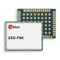
Figure 44: RF input trace
The RF_IN trace on the top layer should be referenced to a suitable ground layer.
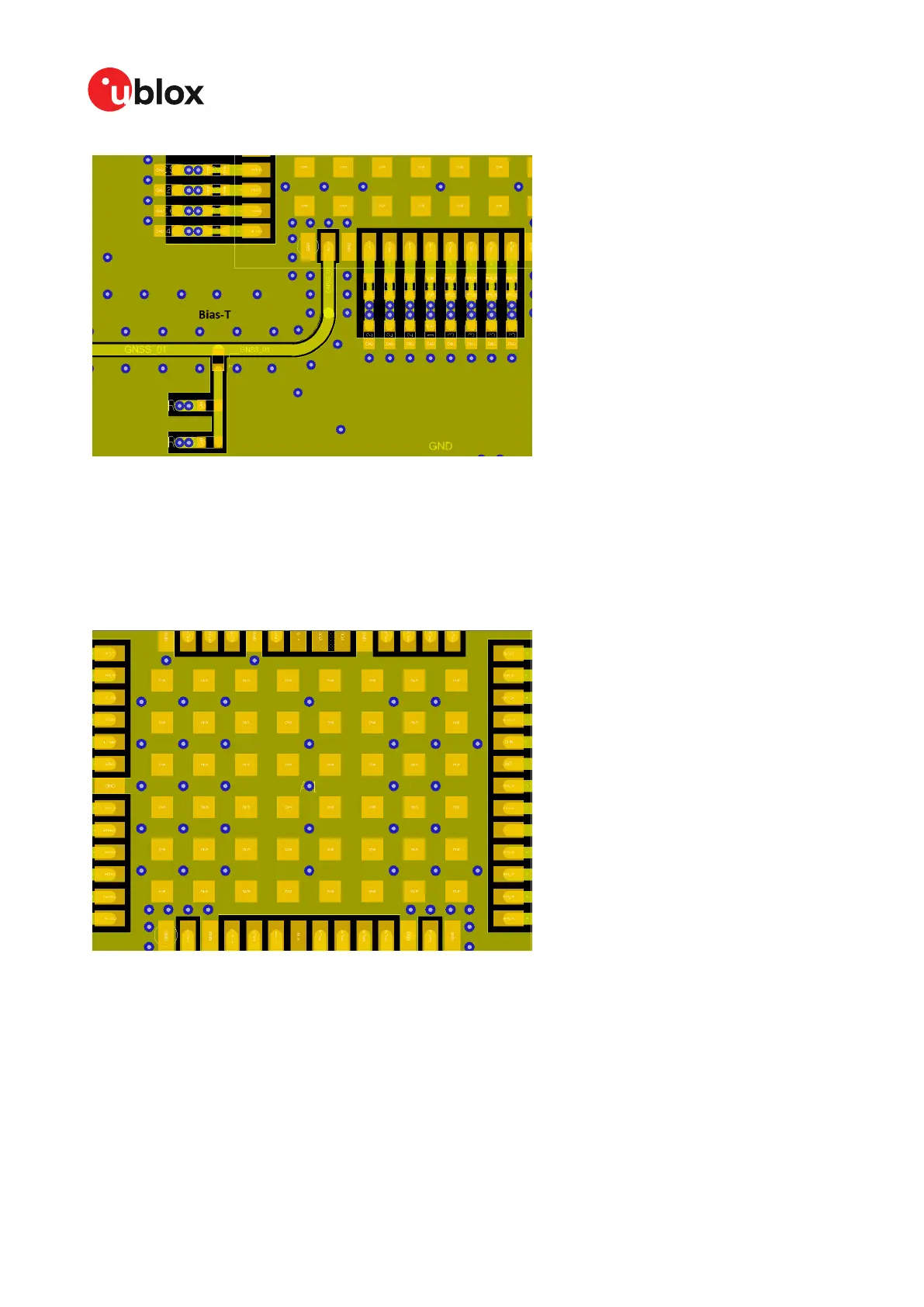
4.8.4.2 Vias for the ground pads
The ground pads under the ZED-F9K high precision receiver need to be grounded with vias to the
lower ground layer of the PCB. A solid ground layer fill on the top layer of the PCB is recommended.
This is shown in the figure below.
Figure 45: Top layer fill and vias
4.8.4.3 VCC pads
The VCC pads for the ZED-F9K high precision receiver must have as low impedance as possible with
large vias to the lower power layer of the PCB. The VCC pads need a large combined pad and the de-
coupling capacitors must be placed as close as possible. This is shown in the figure below.
UBX-20046189 - R01
4 Design Page 87 of 105
C1-Public Early production information
 Loading...


