ZED-F9K-Integration manual
4 Design
This section provides information to help carry out a successful schematic and PCB design
integrating the ZED-F9K.
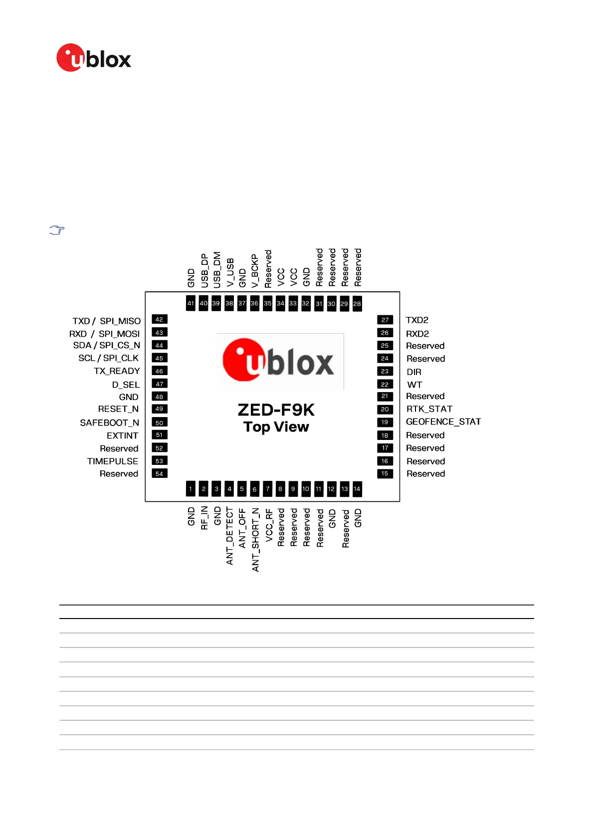
4.1 Pin assignment
The pin assignment of the ZED-F9K module is shown in Figure 31. The defined configuration of the
PIOs is listed in Table 23.
The ZED-F9K is an LGA package with the I/O on the outside edge and central ground pads.
Figure 31: ZED-F9K pin assignment
Pin no. Name I/O Description
1 GND - Ground
2 RF_IN I RF input
3 GND - Ground
4 ANT_DETECT I Active antenna detect
5 ANT_OFF O External LNA disable
6 ANT_SHORT_N I Active antenna short detect
7 VCC_RF O Voltage for external LNA
8 Reserved - Reserved
9 Reserved - Reserved
UBX-20046189 - R01
4 Design Page 72 of 105
C1-Public Early production information
 Loading...