UNION SWITCH & SIGNAL GENISYS II System Hardware Installation
3-16 August 1999 SM-6900B Rev. 0.0
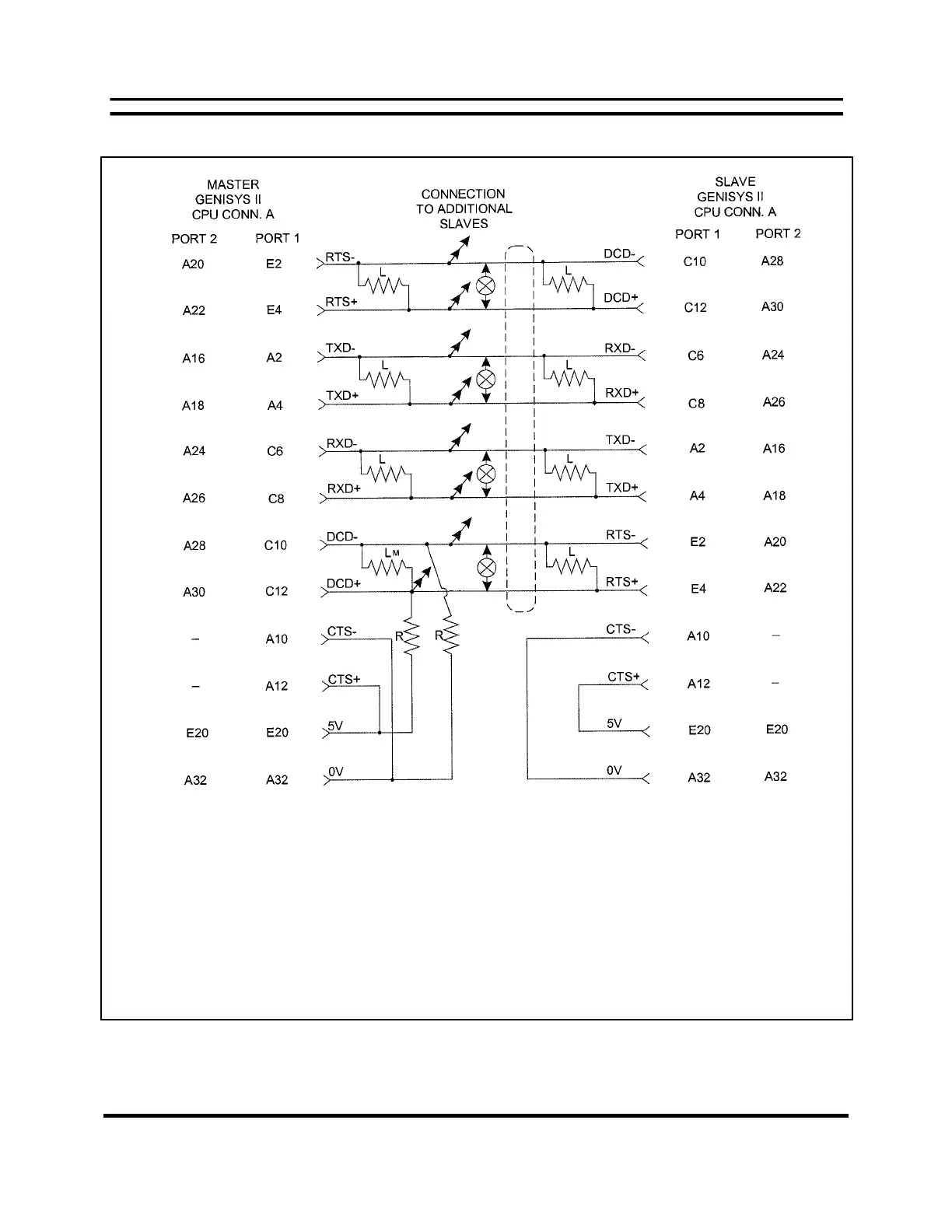
3.4 TYPICAL SERIAL INTERFACE SCHEMATIC DIAGRAMS
1.
DCD biasing resistors (R) are 470 ohm, ½ watt.
2.
For full-duplex Genisys Protocol RTS and DCD need not be connected.
3.
Serial commons are interconnected through the battery that powers the GENISYS II units.
4.
Load resistors (L) are 120 ohm, 1/2 watts and are to be installed externally on the master
and on the most distant slave on the circuit only. Load resistor (Lm) is 240 ohm, ½ watt
and is installed on master DCD only, as shown.
5.
Do not connect serial port common to ground.
F
IGURE
3-3. T
YPICAL
GENISYS II M
ASTER
T
O
GENISYS II S
LAVE
RS-485 D
IRECT
W
IRE
S
ERIAL
I
NTERFACE
U
NITS
P
OWERED
B
Y
S
AME
B
ATTERY
(H
ALF
-D
UPLEX
GENISYS P
ROTOCOL
)
MASTER
SLAVE
GENISYS
II
CONNECTION
GENISYS
II
CPU
CONN.A
TO ADDITIONAL
CPU CONN. A
SLAVES
PORT2
PORT 1
PORT 1
PORT2
A20
E2
)RTS-
DCD-
C10
A28
DCD+
A22
E4
C12
A30
I
TXD-
RXD-
A16
A2
C6
A24
RXD+
A18 A4
C8
A26
I
A24
RXD-
TXD-
A2
C6
A16
A26
TXD+
A4
C8
A18
I
A28
C10
DCD-
RTS-
E2
A20
A30
C12
RTS+
E4
A22
_.,,
A10
CTS-
CTS-
A10
A12
CTS+
c::
A12
E20
E20
5V
V
E20
E20
A32
A32
ov
ov
A32
A32
 Loading...