27
In case of current sinking inputs and current sourcing outputs
11
12
9
10
21
22
31
32
33
34
1
2
26
29
30
23
24
15
16
13
14
27
28
19
20
17
18
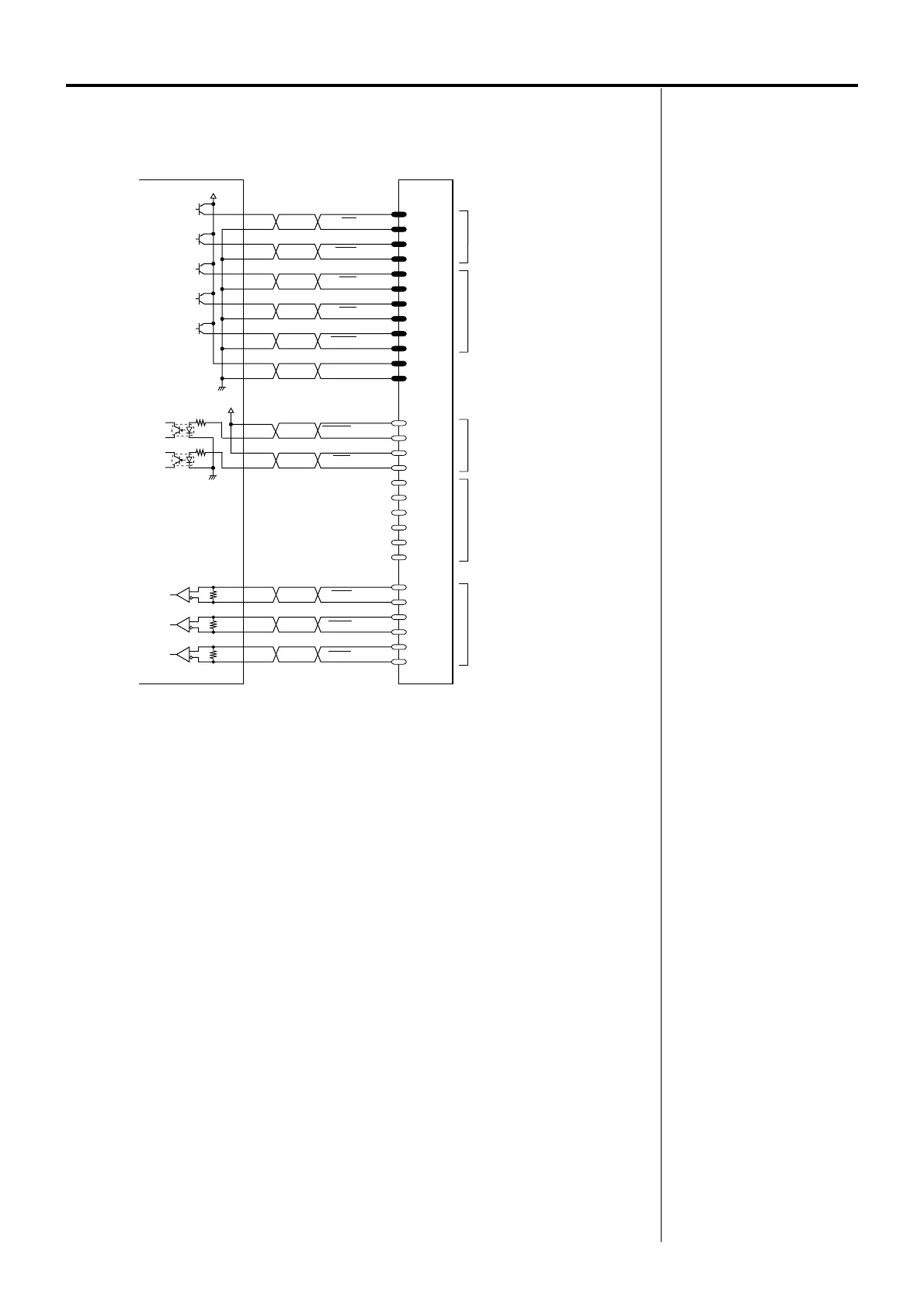
Driver
Controller
CN4
Twisted pair cable
or shielded cable
∗ GND of TIM1, ASG1, BSG1
is common.
The output type of these signals
is current sinking outputs.
See page 39 for the wiring.
+5 V
Photocoupler input
5 VDC Input current 7~20 mA
Photocoupler input
5 VDC Input current 16 mA
Photocoupler/open-collector output
30 VDC, maximum
Output current 15 mA, maximum
Transistor/open-collector output
30 VDC, maximum
Output current 15 mA, maximum
Line-driver output
26C31 or equivalent
CW input
CW input
CCW input
CCW input
ACL input
ACL input
×10 input
×10 input
C.OFF input
C.OFF input
Vcc+5 V input
ALARM output
ALARM output
END output
END output
TIM1 output
GND
BSG1 output
TIM2 output
TIM2 output
ASG2 output
ASG2 output
BSG2 output
BSG2 output
25
GND
ASG1 output
GND
GND
Note
Be sure to use the same voltage
for C.OFF, ×10 and ACL inputs
and TIM1/TIM2, ASG1/ASG2
and BSG1/BSG2 outputs.
Connecting both 5 and 24 VDC
power supplies may damage the
driver and power supplies.
 Loading...