ML605 Hardware User Guide www.xilinx.com 23
UG534 (v1.9) February 26, 2019
Detailed Description
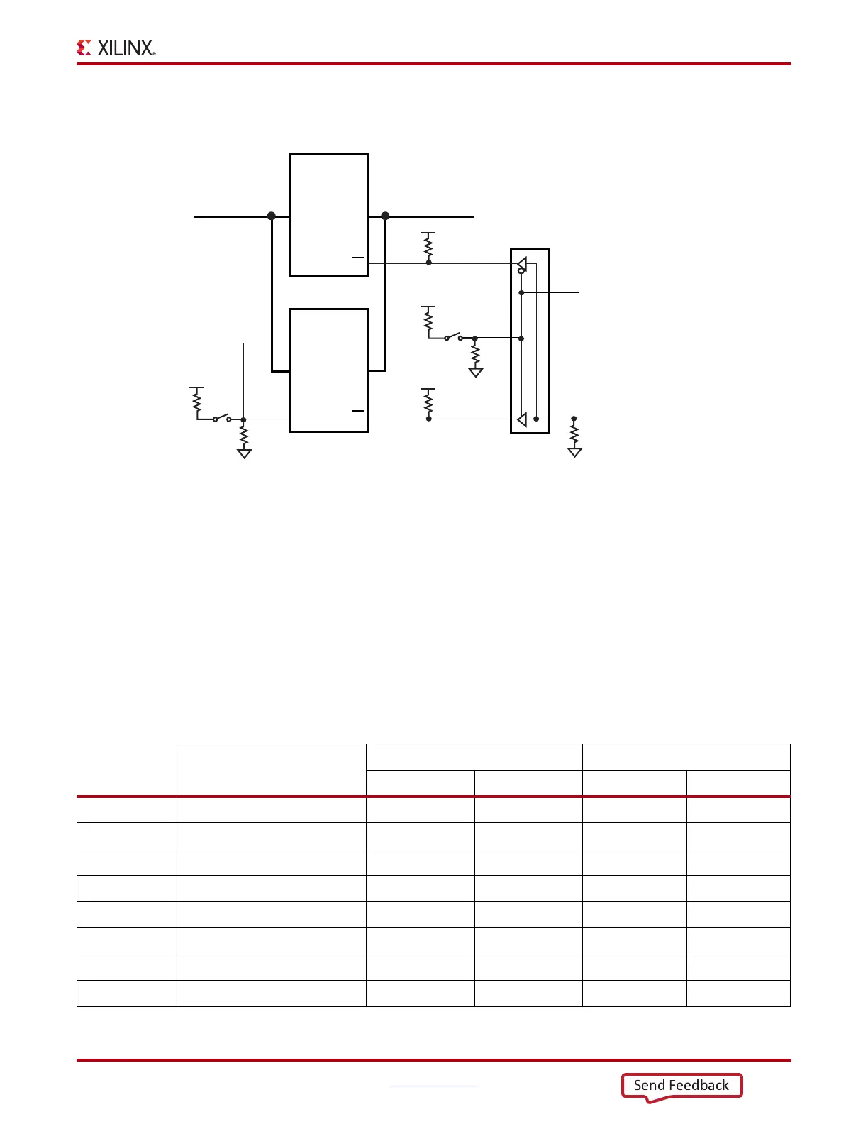
Figure 1-3 shows a block diagram for the Platform Flash and BPI Flash.
ML605 Flash Boot Options
The ML605 has two parallel wired flash memory devices as shown in Figure 1-3. At ML605
power-up, before FPGA configuration, DIP switch S2 switch 2 selects which flash device,
U4 (BPI) or U27 (Platform Flash), provides the boot bitstream. Typically S2 switch 2 will be
open/OFF to select the U27 Platform Flash. Given that the mode switches (S2 switch
3/M0, switch 4/M1 and switch 5/M2) are set to Slave SelectMAP mode, then U27, driven
at 47 MHz, can load a PCIe core bitstream before a host PC motherboard can scan its PCIe
slots. When S2 switch 2 is closed/ON at power up, the FPGA will be configured from the
BPI flash device U4. Note that U4 address bit A23 is switched by S2 switch 6, which allows
the lower or upper half of U4 to be chosen as a data source.
Table 1-5 shows the connections and pin numbers for the boot flash devices.
X-Ref Target - Figure 1-3
Figure 1-3: Platform Flash and BPI Flash Block Diagram
UG534_03_011110
FPGA U1
Bank 34
FLASH_A[22:0]
FPGA U1
Bank 24
FLASH_A[23]
FLASH_D[15:0]
U4
U27
BPI
FLASH
PLATFORM
FLASH
AD
A
A23
D
CE
E
FPGA U1
Bank 24
U10
VCC2V5
VCC2V5
VCC2V5
PLATFLASH_FCS_B
FLASH_CE_B
FPGA_FCS_B
FPGA U1
Bank 24
S2 SWITCH 2
ON = U4 BOOT
OFF = U27 BOOT
1
6
4 3
11
S2-2
2
VCC2V5
7
S2-6510
4.7K
510
4.7K
6
S2 SWITCH 6
ON = U4 BPI Upper Half
OFF = U4 BPI Lower Half
P30_CS_SEL
(FPGA U1 pin AJ12)
S1 Switch 4
OFF = Disable System ACE,
enable U4/U27 flash boot
ON = Enable System ACE boot when
CF card is present
Table 1-5: Platform Flash and BPI Flash Connections
U1 FPGA Pin Schematic Net Name
U4 BPI Flash U27 Platform Flash
Pin Number Pin Name Pin Number Pin Name
AL8 FLASH_A0 29 A1 A1 A00
AK8 FLASH_A1 25 A2 B1 A01
AC9 FLASH_A2 24 A3 C1 A02
AD10 FLASH_A3 23 A4 D1 A03
C8 FLASH_A4 22 A5 D2 A04
B8 FLASH_A5 21 A6 A2 A05
E9 FLASH_A6 20 A7 C2 A06
E8 FLASH_A7 19 A8 A3 A07