ML605 Hardware User Guide www.xilinx.com 17
UG534 (v1.9) February 26, 2019
Detailed Description
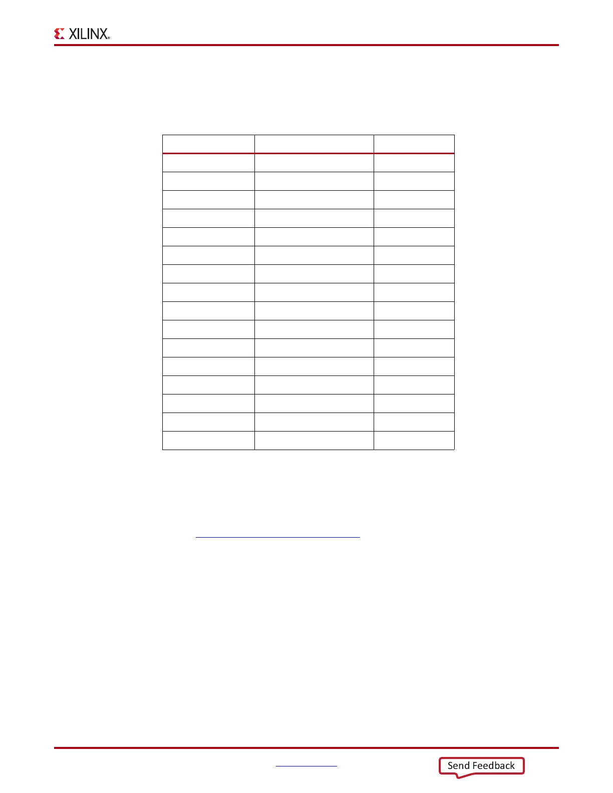
I/O Voltage Rails
There are 16 I/O banks available on the Virtex-6 device. The voltage applied to the FPGA
I/O banks used by the ML605 board is summarized in Table 1-3.
See the X
ilinx Virtex-6 FPGA documentation for more information.
2. 512 MB DDR3 Memory SODIMM
The ML605 204-pin 1.5V SODIMM socket J1 supports up to 2 GB SODIMMs. The ML605 is
delivered with a 512 MB DDR3 SODIMM for user applications.
•Manufacturer: Micron
• Part Number: MT4JSF6464HY-1G1B1
•Description:
• 512 MB (64 Mb x 64)
• 1.5V 204-pin
• Performance: up to DDR3-1066
Table 1-3: Voltage Rails
U1 FPGA Bank I/O Rail Voltage
Bank 0 VCC2V5_FPGA 2.5V
Bank 12
(1)
FMC_VIO_B_M2C 2.5V
Bank 13 VCC2V5_FPGA 2.5V
Bank 14 VCC2V5_FPGA 2.5V
Bank 15 VCC2V5_FPGA 2.5V
Bank 16 VCC2V5_FPGA 2.5V
Bank 22 VCC2V5_FPGA 2.5V
Bank 23 VCC2V5_FPGA 2.5V
Bank 24 VCC2V5_FPGA 2.5V
Bank 25 VCC1V5_FPGA 1.5V
Bank 26 VCC1V5_FPGA 1.5V
Bank 32 VCC2V5_FPGA 2.5V
Bank 33 VCC2V5_FPGA 2.5V
Bank 34 VCC2V5_FPGA 2.5V
Bank 35 VCC1V5_FPGA 1.5V
Bank 36 VCC1V5_FPGA 1.5V
Notes:
1. The VITA 57.1 specification stipulates that the Bank 12 voltage named
FMC_VIO_B_M2C is supplied by the FMC card plugged onto the relevant
FMC connector (ML605 J64). FMC_VIO_B_M2C cannot exceed the base
board (ML605) Vadj of the FMC connector. The ML605 FMC Vadj
maximum is 2.5V.