18 www.xilinx.com ML605 Hardware User Guide
UG534 (v1.9) February 26, 2019
Chapter 1: ML605 Evaluation Board
The ML605 XC6SVX240T FPGA DDR memory interface performance is documented in the
Virtex-6 FPGA Data Sheet: DC and Switching Characteristics (DS152) [Ref 4].
The ML605 DDR3 64-bit wide interface has been tested to 800 MT/s.
The DDR3 interface is implemented in FPGA banks 25, 26, 35, and 36. DCI VRP/N resistor
connections are only implemented banks 26 and 36. DCI functionality in banks 25 and 35 is
achieved in the UCF by cascading DCI between adjacent banks as follows:
CONFIG DCI_CASCADE = "36 35";
CONFIG DCI_CASCADE = "26 25";
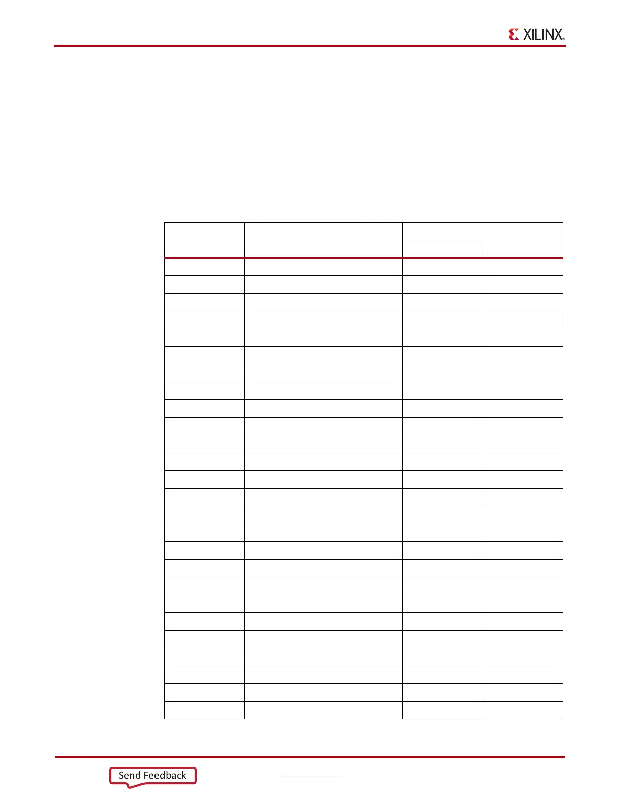
Table 1-4 shows the connections and pin numbers for the DDR3 SODIMM.
Table 1-4: DDR3 SODIMM Connections
U1 FPGA Pin Schematic Net Name
J1 SODIMM
Pin Number Pin Name
L14 DDR3_A0 98 A0
A16 DDR3_A1 97 A1
B16 DDR3_A2 96 A2
E16 DDR3_A3 95 A3
D16 DDR3_A4 92 A4
J17 DDR3_A5 91 A5
A15 DDR3_A6 90 A6
B15 DDR3_A7 86 A7
G15 DDR3_A8 89 A8
F15 DDR3_A9 85 A9
M16 DDR3_A10 107 A10/AP
M15 DDR3_A11 84 A11
H15 DDR3_A12 83 A12_BC_N
J15 DDR3_A13 119 A13
D15 DDR3_A14 80 A14
C15 DDR3_A15 78 A15
K19 DDR3_BA0 109 BA0
J19 DDR3_BA1 108 BA1
L15 DDR3_BA2 79 BA2
J11 DDR3_D0 5 DQ0
E13 DDR3_D1 7 DQ1
F13 DDR3_D2 15 DQ2
K11 DDR3_D3 17 DQ3
L11 DDR3_D4 4 DQ4
K13 DDR3_D5 6 DQ5