ML605 Hardware User Guide www.xilinx.com 37
UG534 (v1.9) February 26, 2019
Detailed Description
The PCIe interface obtains its power from the DC power supply provided with the ML605
or through the 12V ATX power supply connector. The PCIe edge connector is not used for
any power connections.
The board can be powered by one of two 12V sources; J60, a 6-pin (2x3) molex-type
connector; and J25, a 4-pin (inline) ATX disk drive type connector.
The 6-pin molex-type connector provides 60W (12V @ 5A) from the AC power adapter
provided with the board while the 4-pin ATX disk drive connector is provided for users
who want to power their board while it is installed inside a PC chassis.
For applications requiring additional power, such as the use of expansion cards drawing
significant power, a larger AC adapter might be required. If a different AC adapter is used,
its load regulation should be better than ±10%.
ML605 power switch SW2 turns the board on and off by controlling the 12V supply to the
board.
Caution!
Never apply power to the power brick connector (J60) and the 4-pin ATX disk drive
connector (J25) at the same time as this will result in damage to the board. See Figure 1-23.
Never connect an auxiliary PCIe 6-pin molex power connector to J60 6-pin molex on the ML605
board as this could result in damage to the PCIe motherboard and/or ML605 board. The 6-pin
molex connector is marked with a no PCIe power label to warn users of the potential hazard.
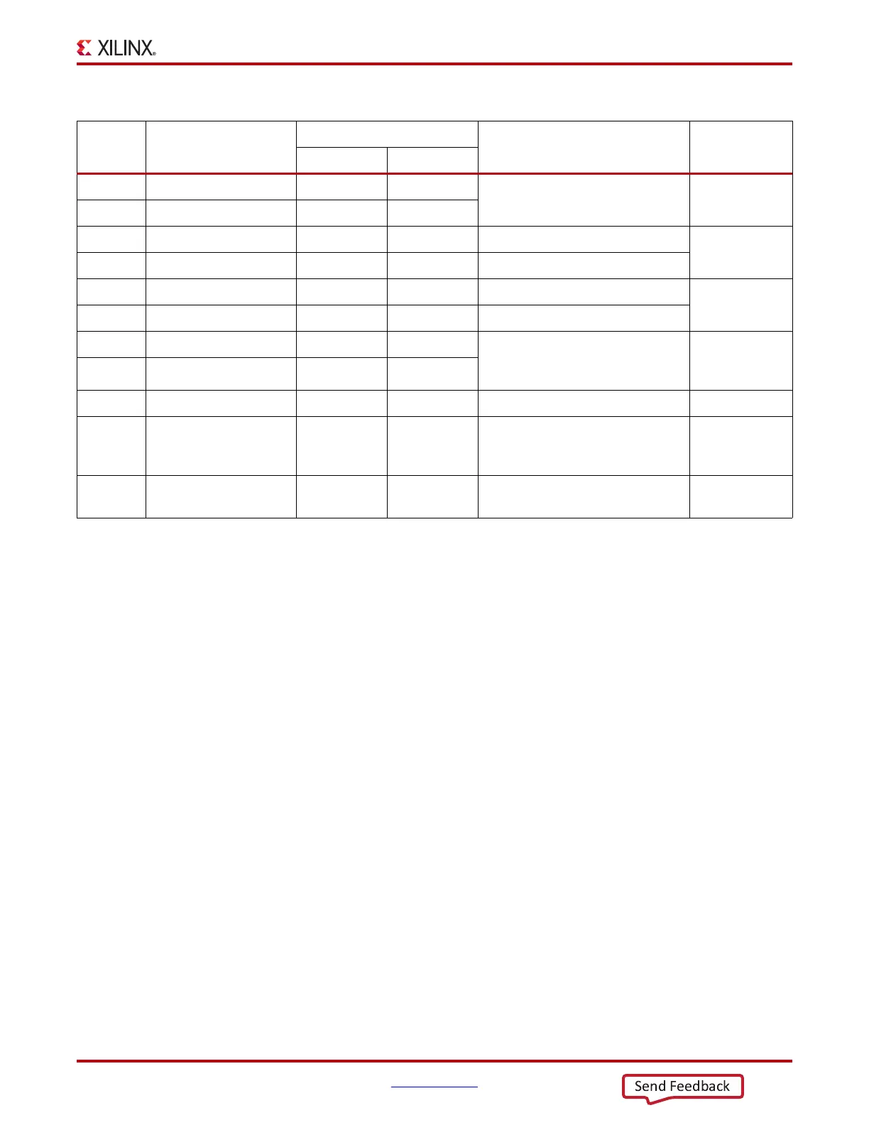
AA3 PCIE_RX7_P B45 PETp7
Integrated Endpoint block
receive pair
GTXE1_X0Y8
AA4 PCIE_RX7_N B46 PETn7
P6 PCIE_100M_MGT0_P U14.16 Q0 Sourced from U14 ICS854104
IBUF_
GTXE1_X0Y6
P5 PCIE_100M_MGT0_N U14.15 NQ0 clock driver
V6 PCIE_250M_MGT1_P U9.18 Q Sourced from U9 ICS874001
IBUF_
GTXE1_X0Y4
V5 PCIE_250M_MGT1_N U9.17 NQ clock multiplier/driver
U14.6 PCIE_CLK_QO_P A13 REFCLK+ Integrated Endpoint block
differential clock pair from PCIe
edge connector
U14.7 PCIE_CLK_QO_N A14 REFCLK-
J42.2,4,6 PCIE_PRSNT_B A1 PRSNT#1 J42 Lane Size Select jumper
AD22 PCIE_WAKE_B B11 WAKE#
Integrated Endpoint block wake
signal, not connected on ML605
board
AE13 PCIE_PERST_B A11 PERST
Integrated Endpoint block reset
signal
Notes:
1. PCIE_TXn_P/N pairs are capacitively coupled to FPGA
2. PCIE_100M_MGT0_P/N pairs are capacitively coupled to FPGA
3. PCIE_250M_MGT1_P/N pairs are capacitively coupled to FPGA
4. PCIE_PERST_B is level-shifted by U32
5. For ML605, access is through MGT Banks 114 and 115
Table 1-8: PCIe Edge Connector Connections (Cont’d)
U1 FPGA
Pin
Schematic Net Name
P1 PCIe Edge Connector
Description
Package
Placement
Pin Number Pin Name