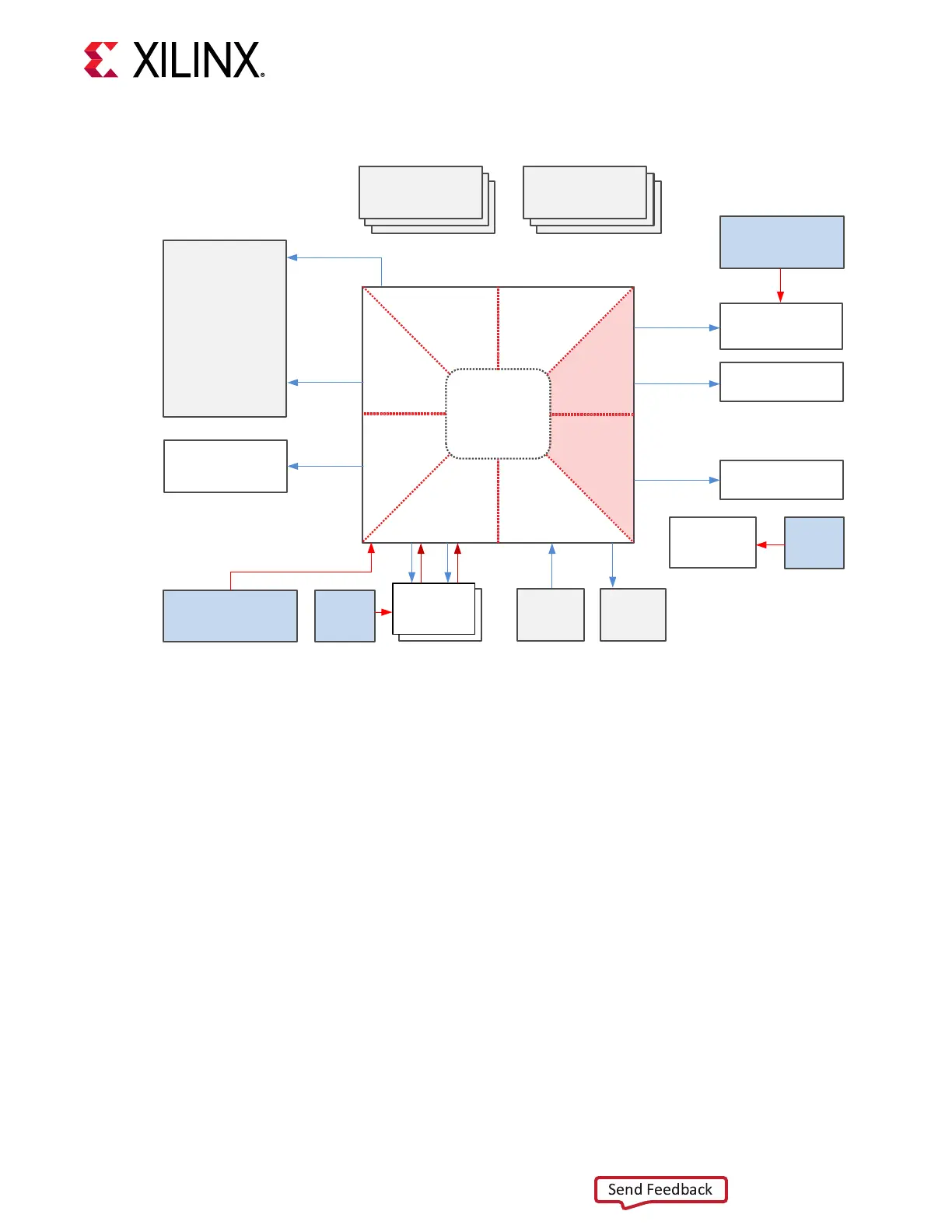
Figure 7: SP701 Clocking Diagram
25 MHz
Crystal
MIPI-
Camera
Conn
Bank13
Bank14
Bank15
Bank16
Bank34
Bank35
Bank33
Bank36
DDR3
4Gbit x16
ADV7511
HDMI Transmitter
SIT8102
12 MHz Osc
FMC LPC Connector
68 I/Os
Pmod x3
12pin Female
SPI NOR Flash
EEPROM
MIPI-Display
Conn
XADC
XADC
Config
DSI_CLK_P/N
12MHz
Config
FT4232H
USB to
UART/JTAG
Pmod x3
12pin Female
IDCK_P/N
12 MHz
I2C_SCL
FLASH_CLK
OSCI
CSI_CLK_P/N
DP838671R
10/100/100
PHY
TCK
RCK
TCK
RCK
25 MHz
Crystal
CLK_INOUT
10 MHz-810 MHz
Si570
SYS_CLK_P/N
CK_P/N
FMC_CLK1_P/N
2X CLK
FMC_CLK0_P/N
2X CLK
X22790-050319
USB UART Interface
[Figure 2, callout 13]
The FT4232HQ U6 mulfuncon USB-UART on the SP701 board provides two level-shied
UART connecons through the single micro-AB USB connector J5.
• Channel ADBUS is congured in JTAG mode to support the JTAG chain
• Channel ACBUS implements 4-wire FT4232_B_UART (level-shied) FPGA U1 bank 14
connecons
• Channel BDBUS implements 4-wire FT4232_C_UART (level-shied) FPGA U1 bank 13
connecons
• Channel BCBUS implements 2-wire FT4232_D_UART MSP430 U25 connecons
The USB UART interface circuit is shown in the following gure.
Chapter 3: Board Component Descriptions
UG1319 (v1.0) July 12, 2019 www.xilinx.com
SP701 Board User Guide 22