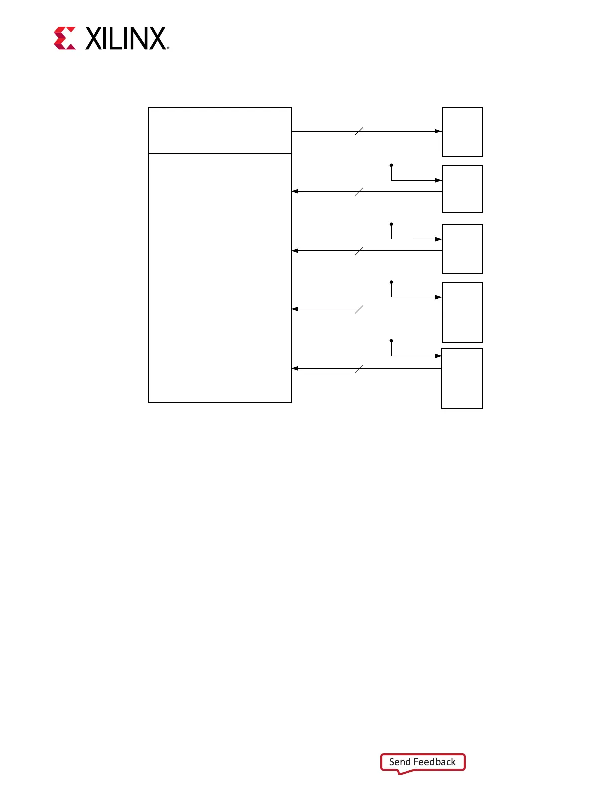
Figure 16: User GPIO
Bank 13
Vcco = 1.8V
Spartan-7 FPGA
Bank 15
Vcco = 3.3V
8X LED
(Green)
8-pole
DIP SW
8-pole
DIP SW
5x Pushbutton
N,W,C,E,S
(active-High)
1x Pushbutton
CPU_RESET
(active-High)
1.8V
1.8V
1.8V
1.8V
GPIOx1
GPIOx5
GPIOx8
GPIOx8
GPIOx8
X22798-050319
The detailed FPGA connecons for the feature described in this secon are documented in the
SP701 board XDC le, referenced in Appendix B: Xilinx Design Constraints.
User PMOD GPIO Connectors
[Figure 2, callout 20, 21]
The SP701 evaluaon board implements six right-angle PMOD GPIO receptacles J14-J19. The
3.3V PMOD nets are wired to the XC7S100 FPGA 3.3V bank 16. For more informaon about
PMOD connector compable PMOD modules, see the Digilent Inc. website.
The following gure shows the GPIO PMOD connectors.
Chapter 3: Board Component Descriptions
UG1319 (v1.0) July 12, 2019 www.xilinx.com
SP701 Board User Guide 33