EasyManuals Logo
Home>Xilinx>Motherboard>SP701

Xilinx SP701 User Manual

Xilinx SP701
50 pages
To Next Page IconTo Next Page
To Previous Page IconTo Previous Page
Page #38 background imageLoading...
Page #38 background image
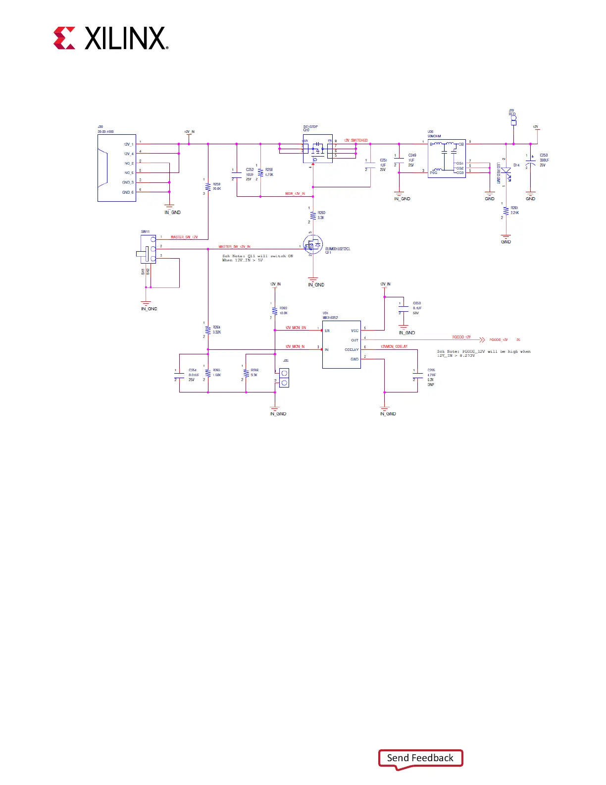
Figure 20: SP701 Power Input
Board Power System
[Figure 2, callout 29]
The SP701 power system is comprised of monolithic power systems components. The four
outputs (VCCINT, VCCO_1V8, VCCO_2V5, and VCCO_3V3) of the MP5470 U34 regulator are
adjustable through its I2C bus connecon accessible from the FPGA U1 Bank 16 and the
MSP430 system controller.
The following gure shows the SP701 power system block diagram.
Chapter 3: Board Component Descriptions
UG1319 (v1.0) July 12, 2019 www.xilinx.com
SP701 Board User Guide 38
Send Feedback

Other manuals for Xilinx SP701

Questions and Answers:

Question and Answer IconNeed help?

Do you have a question about the Xilinx SP701 and is the answer not in the manual?

Xilinx SP701 Specifications

General IconGeneral
BrandXilinx
ModelSP701
CategoryMotherboard
LanguageEnglish

Related product manuals