Figure 21: Power System Block Diagram
1
4
2
5
3
6
12V External
Connector
39-30-1060
Power
Noise Filter
MP8756
Input: 4.5V-26V
6A Buck
1V @ 2.5A
6A
2A
6A
3.3V AUX for FMC
1.8V @ 2A
FPGA VCCINT
FPGA, 2x DP83867,
ADV7511, UI
3A
0.8A
0.65A
2A
0.04A
FMC-LPC
1A
1V
1.05V
12V
12.6V
2.5V
2.625V
VADJ
1.8V to 3.465V
3.3V/3A for MIPI
Display & Camera
3A
12V
12.6V
3.3V
3.465V
1.35V
1.43V
3.3V
3.465V
5V
5.25V
2.5 @ 1A
FPGA VCCIO, 2x
DP83867 IO
3.3V @ 1.5A
FPGA, FLASH,
EEPROM, FT4232, UI
& 6xPmod
3A
3A
2A
2A
1.35V @ 0.6A
FPGA & DRAM
MP8756
Input: 4.5V-26V
6A Buck
MPM3620A
Input: 4.5V-26V
2A Buck
3.3V
3.465V
3.3V @ 0.1A
MPM3606A
Input: 4.5V-21V
0.6A Buck
0.08A
5V @ 0.15A
HDMI Conn
VIN1
VIN2
0.08A
1A
1.1A
1.6A
3.3V
3.465V
1.8V
1.89V
MPM3805
Input: 2.5V-6B
0.6A Buck
2x DP83867IR Core
(2x 125mA)
1.1V
MP20073
Input: 1.3V-6V
2A VTT-LDO
VTT_0V675
DDR3L
0.675V
MPM3620A
Input: 4.5V-24V
2A Buck
Current Monitor
Current
Monitor
MP5470
Input : 4V-16
Output : 0.55V-5.46V
3A/3A/2A/2A Buck
X22801-050319
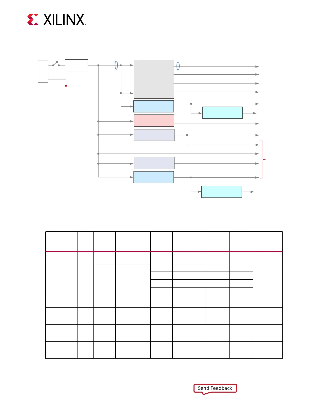
The following table lists the SP701 power system voltage regulators.
Table 12: SP701 Power System
Device Type
Ref.
Des.
I2C
Address
Description O/P
Power Rail
Net Name
Power
Rail
Voltage
Max.
Current
Schematic
Page
INA226AIDGS U32
0x41
Current and
power monitor
N/A 12V N/A N/A 24
MP5470GL U34
0x68
Four-output
PMIC
SW1 VCCINT_1V 1.00V 3A 24
SW2 VCCO_1V8 1.80V 2A
SW3 VCCO_2V5 2.50V 2A
SW4 VCCO_3V3 3.30V 2A
INA226AIDGS U33
0x44
Current and
power monitor
N/A VCCINT_1V N/A N/A 24
MPM3620A U35 N/A Synchronous
step-down
converter
OUT VCCO_1V35 1.35V 2A 25
MPM3606A U36 N/A Synchronous
step-down
converter
OUT 5V 5.0V 0.6A 25
MPM3805GQB U38 N/A Synchronous
step-down
converter
OUT 1V1_VDD 1.10V 0.6A 25
Chapter 3: Board Component Descriptions
UG1319 (v1.0) July 12, 2019 www.xilinx.com
SP701 Board User Guide 39