Table 12: SP701 Power System (cont'd)
Device Type
Ref.
Des.
I2C
Address
Description O/P
Power Rail
Net Name
Power
Rail
Voltage
Max.
Current
Schematic
Page
MPM3620A U37 N/A Synchronous
step-down
converter
OUT 3V3AUX 3.30V 2A 25
MP8756GD U39 N/A POL switching
regulator
SW 3V3_EXT 3.30V 6A 26
MP8756GD U40 N/A POL switching
regulator
SW VADJ 1.80V 6A 26
MP20073DH U13 N/A DDR memory
termination
regulator
VTTREF VTTREF 0.675V 2A 6
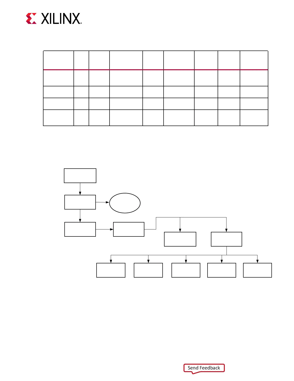
The following gure shows the SP701 power system sequencing diagram.
Figure 22: Power System Sequence
POWER UP SEQUENCE
12V
3V3AUX
SYS CTRL
MSP430
VCCINT_1V VCCO_1V8
VCCO_2V5 VCCO_3V3
VCCO_1V35 1V1_VDD 5V 3V3_EXT VADJ
X22953-061119
The opons for VADJ are 1.8V, 2.5V, and 3.3V. They can be selected using the System Controller
(MSP430) I2C connected TCA64164A I/O expander U24 ports P06 VSEL0_VADJ and P07
VSEL1_VADJ pins. The VADJ regulator can similarly be powered ON/OFF by the TCA64164A
I/O expander U24 port P04 pin.
Chapter 3: Board Component Descriptions
UG1319 (v1.0) July 12, 2019 www.xilinx.com
SP701 Board User Guide 40