VCU1525 Acceleration Platform User Guide 13
UG1268 (v1.0) November 13, 2017 www.xilinx.com
Chapter 2: Board Setup and Configuration
At power up, the FPGA is configured by the Quad SPI NOR Flash U17 device (Micron
MT25QU01GBBA8E12-0SIT) with the FPGA_CCLK operating at clock rate of 105 MHz
(EMCCLK) using the Master Serial Configuration mode.
The Quad SPI flash memory NOR device has a capacity of 1 Gb.
While the FPGA default mode selects Quad SPI configuration, JTAG mode overrides it if
invoked. JTAG mode is always available independent of the Mode pin settings.
M0 is pulled up, however it is also connected to the I2C I/O port U2 PCA9536 device (port
P1, pin 2). This connection allows M0 to be driven low by the MSP432 U19 BMC over I2C (via
the I2C PCS9536 U2 port expander), disabling the Master SPI mode.
For complete details on configuring the FPGA, see UltraScale Architecture Configuration
User Guide (UG570) [Ref 1].
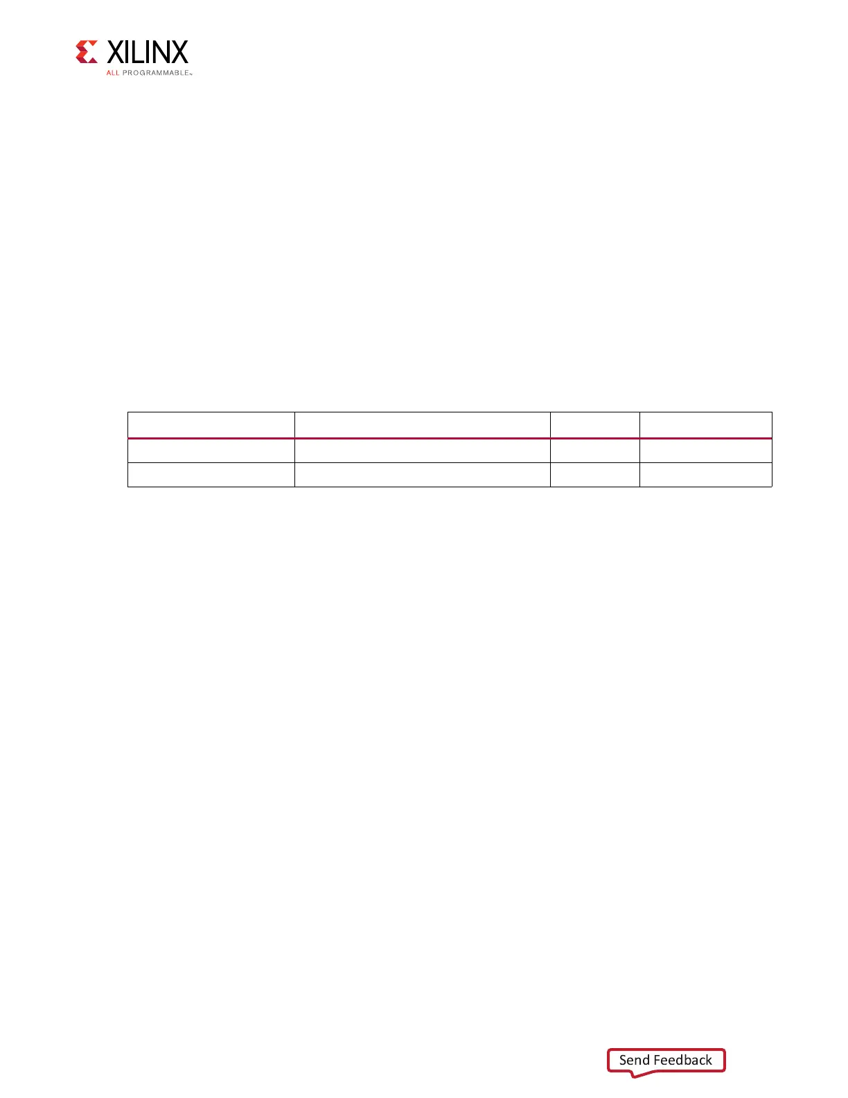
Table 2-4: Configuration Modes
Configuration Mode M[2:0] Bus Width CCLKL Direction
Master SPI 001 x1, x2, x4 FPGA output
JTAG Not applicable - JTAG overrides x1 Not applicable