VCU1525 Acceleration Platform User Guide 7
UG1268 (v1.0) November 13, 2017 www.xilinx.com
Chapter 1: Introduction
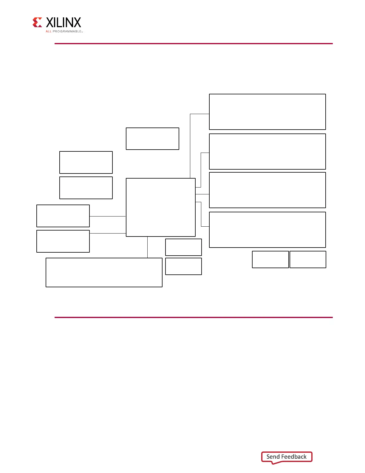
Block Diagram
A block diagram of the VCU1525 board is shown in Figure 1-3.
Board Features
The VCU1525 board features are listed in this section. Detailed information for each feature
is provided in Component Descriptions in Chapter 3.
• Virtex UltraScale+ XCVU9P-L2FSGD2104E FPGA
• Memory (four independent dual-rank DDR4 interfaces)
°
48 gigabyte (GB) DDR4 memory
°
4x DDR4 16 GB, 2400 mega-transfers per second (MT/s), 64-bit with error correcting
code (ECC) DIMM
X-Ref Target - Figure 1-3
Figure 1-3: VCU1525 Board Block Diagram
244-pin DIMM interface
64-bit + ECC dual rank support
x4/x8 UDIMM support
PC4-2400 compatible
C0
244-pin DIMM interface
64-bit + ECC dual rank support
x4/x8 UDIMM support
PC4-2400 compatible
C2
244-pin DIMM interface
64-bit + ECC dual rank support
x4/x8 UDIMM support
PC4-2400 compatible
C3
244-pin DIMM interface
64-bit + ECC dual rank support
x4/x8 UDIMM support
PC4-2400 compatible
C1
DIP SW POWER
QSPI1
QSPI2
PCIe GEN1/2/3 x 1/2/4/8/16
PCIe GEN4 x 8
QSFP #2
QSFP #1
XADC
LEDs
Clocks
VU9P
D2104
X19964-110617