VCU1525 Acceleration Platform User Guide 28
UG1268 (v1.0) November 13, 2017 www.xilinx.com
Chapter 3: Board Component Descriptions
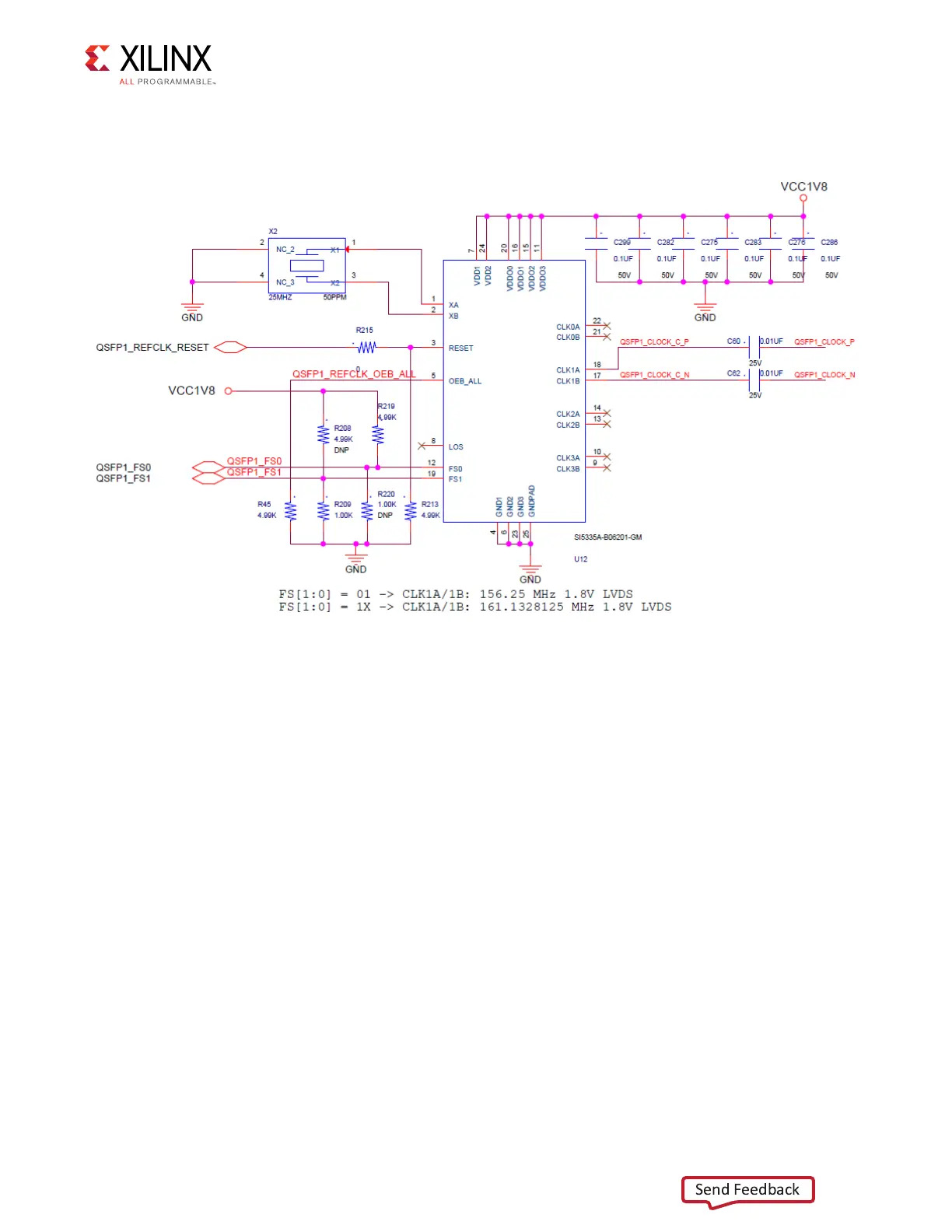
The QSFP1 Si5335A U12 clock circuit is shown in Figure 3-8.
Programmable MGT and User Clock
[Figure 2-1, callout 12]
The VCU1525 board has an SI570 programmable low-jitter 3.3V LVDS differential oscillator
(U14) connected to a SI53340 (U43) 1-to-4 LVDS clock buffer.
On power-up, the SI570 user clock defaults to an output frequency of 156.250MHz. User
applications can change the output frequency within the range of 10MHz to 810 MHz
through an inter IC (I2C) interface. Power cycling the VCU1525 board resets this clock to the
default frequency of 156.250MHz.
• Programmable oscillator: Silicon Labs Si570BAB0000544DG (10MHz–810MHz)
• Frequency jitter: 50 ppm
• 3.3V LVDS differential output
• Default frequency 156.250MHz
• I2C address 0x5D
X-Ref Target - Figure 3-9
Figure 3-9: QSFP1 156.25MHz Clock Circuit