VCU1525 Acceleration Platform User Guide 22
UG1268 (v1.0) November 13, 2017 www.xilinx.com
Chapter 3: Board Component Descriptions
Table 3-3 lists the USB switch circuit connections.
The FTDI FT4232HQ data sheet is available on the FTDI website [Ref 6].
The TS3USB221RSER data sheet is available on the TI website [Ref 8].
Clock Generation
[Figure 2-1, callout 10, 11, 12]
The VCU1525 board provides eight clock sources to the XCVU9P-L2FSGD2104E device,
listed in Table 3-4.
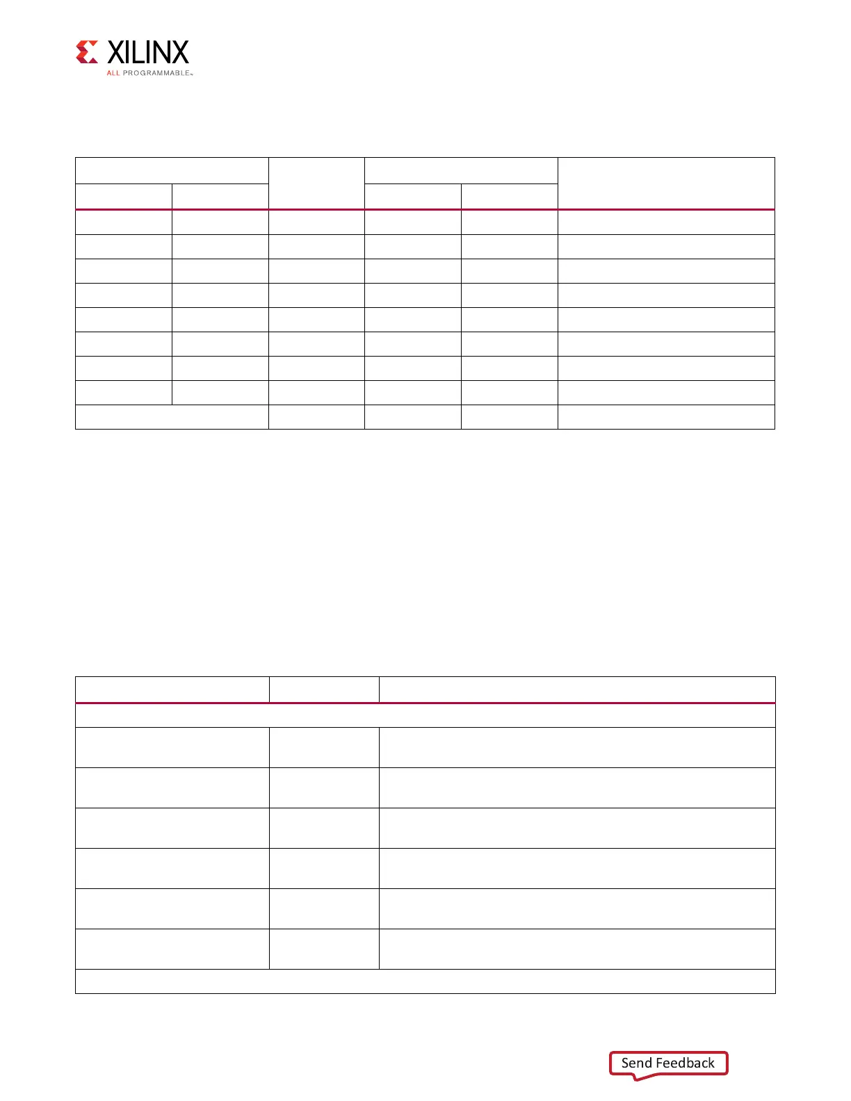
Table 3-3: VCU1525 USB Switch Circuit Connections
TS3USB221RSER U59
Schematic
Net Name
Connected To
Description
Pin Pin Name Pin Name
1 1D+ USB1_DP J13.3 D_P USB J13 DP
2 1D- USB1_DN J13.2 D_N USB J13 DN
3 2D+ USB2_DP J17.2 2 USB J17 DP
4 2D- USB2_DN J17.3 3 USB J17 DN
6 OE_B USB_EN_B U19.52 P9_0 U59 USB Switch ENABLE_B
7 D- USB_DN U27.7 DM FT4232HQ U27 DN
8 D+ USB_DP U27.8 DP FT4232HQ U27 DP
9 S USB_SEL U19.53 P9_1 U59 USB Switch Port Select
J17 USB_VBUS2 present USB_PRES U19.24 P10_4 USB J17 pin 1 voltage detection
Table 3-4: VCU1525 Board Clock Sources
Clock Name Clock Ref. Des. Description
SYSCLK_300 clock buffer U44 source is SI5335A-B06201-GM U9 output CLK0 (300MHz).
DDR4 C0 I/F 300MHz U44 (Q0) Silicon Labs Si53340 3.3V LVDS clock buffer. SYSCLK0_300_P/N
DDR4 C0 I/F bank 63.
DDR4 C1 I/F 300MHz U44 (Q1) Silicon Labs Si53340 3.3V LVDS clock buffer. SYSCLK1_300_P/N
GPIO I/F bank 64.
DDR4 C2 I/F 300MHz U44 (Q2) Silicon Labs Si53340 3.3V LVDS clock buffer. SYSCLK2_300_P/N
DDR4 C2 I/F bank 70.
DDR4 C3 I/F 300MHz U44 (Q3) Silicon Labs Si53340 3.3V LVDS clock buffer. SYSCLK3_300_P/N
DDR4 C3 I/F bank 72.
QSFP0 CLOCK 156.250MHz U9 (CLK1) Silicon Labs Si5335A 1.8 LVDS QSFP0_CLOCK_P/N QSFP0
GTY231 REFCLK1
QSFP1 CLOCK 156.250MHz U12 (CLK1) Silicon Labs Si5335A 1.8 LVDS QSFP1_CLOCK_P/N QSFP1
GTY230 REFCLK1
USER/MGT_SI570_CLOCK buffer U43 source is SI570 U14 (156.250MHz default).