VCU1525 Acceleration Platform User Guide 23
UG1268 (v1.0) November 13, 2017 www.xilinx.com
Chapter 3: Board Component Descriptions
The FPGA connections for each clock are listed in Appendix A, Master Constraints File
Listing.
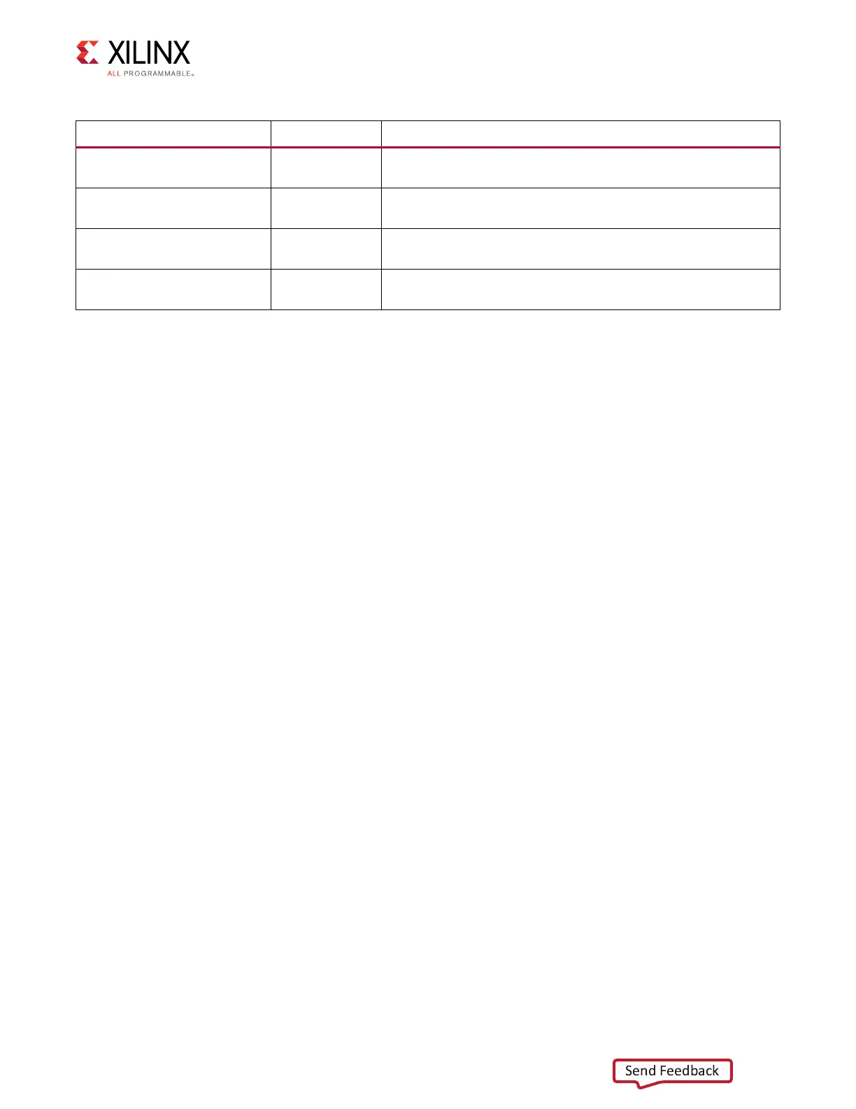
USER_SI570_CLOCK U43 (Q0) Silicon Labs Si53340 3.3V LVDS clock buffer.
USER_SI570_CLOCK_P/N GPIO I/F bank 64.
MGT SI570 CLOCK0 (QSFP0) U43 (Q2) Silicon Labs Si53340 3.3V LVDS clock buffer.
USER_SI570_CLOCK0_P/N QSFP0 GTY231 REFCLK0.
MGT SI570 CLOCK1 (QSFP1) U43 (Q3) Silicon Labs Si53340 3.3V LVDS clock buffer.
USER_SI570_CLOCK0_P/N QSFP1 GTY230 REFCLK0.
PEX_REFCLK (PCIe input) CN1 PCIe edge conn. CN1 input clock 100MHz PEX_REFCLK_P/N
GTY226 REFCLK0.
Table 3-4: VCU1525 Board Clock Sources (Cont ’d)
Clock Name Clock Ref. Des. Description