VCU1525 Acceleration Platform User Guide 12
UG1268 (v1.0) November 13, 2017 www.xilinx.com
Chapter 2: Board Setup and Configuration
Default Switch Settings
Default switch settings are listed in Table 2-2. Switch locations are shown in Figure 2-1.
Table 2-3 shows other visible switch locations.
Installing the VCU1525 Board in a Server Chassis
Follow the server manufacturer's instructions for add-in board installation.
FPGA Configuration
The VCU1525 board supports two UltraScale+ FPGA configuration modes:
• Quad SPI flash memory
• JTAG using USB JTAG configuration port (USB J13/FT4232H U27)
The FPGA bank 0 mode pins are hardwired to M[2:0] = 001 Master SPI mode with
pull-up/down resistors.
15 U19 Board Management Controller
(BMC)
TI MSP432P401RIPZ 24
16 JP1 Auxiliary 12V power connector
(Vccint Regulator Circuit)
LIGHT JIE AARRA001-08MTTRH 17
17 J4 Cooling Fan Connector JST SALES S4B-PH-K-S(LF)(SN) 11
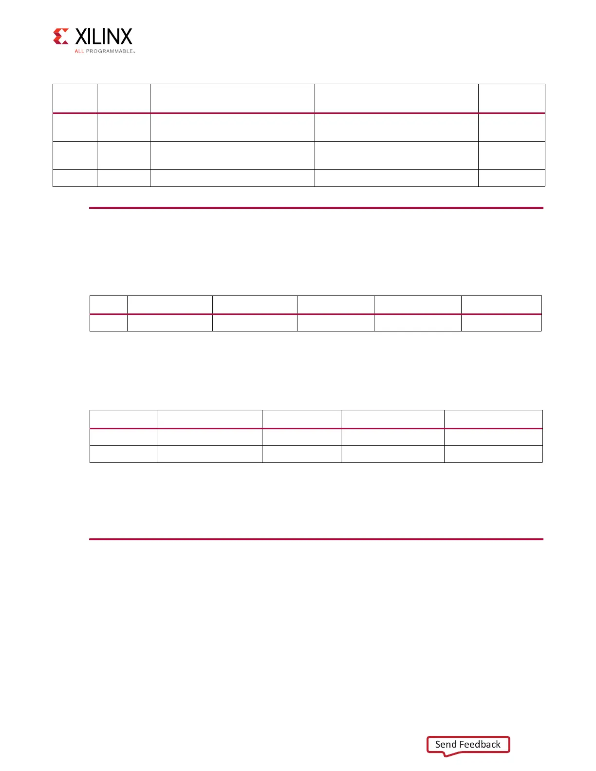
Table 2-1: VCU1525 Board Component Descriptions (Cont’d)
Number Ref Des
Feature
(Link)
Notes
Schematic
Page
Table 2-2: Default Switch Settings
Switch Function Default Comments Figure 2-1 Callout Schematic Page
SW3
(1)
4-pole GPIO DIP ON, ON, ON, ON 4-pole user DIP 18 11
Notes:
1. On revision D and later boards, this switch is not populated.
Table 2-3: Other Visible Switches
Component Function Comments Figure 2-1 Callout Schematic Page
SW1 Pushbutton switch CPU_RESET_B 19 11
SW2 Pushbutton switch PROGRAM_B 20 11