VCU1525 Acceleration Platform User Guide 21
UG1268 (v1.0) November 13, 2017 www.xilinx.com
Chapter 3: Board Component Descriptions
The channel BD UART connection from XCVU9P-L2FSGD2104E U13 bank 64 to the
FT4232HQ U27 device is level-shifted via Q36 (TX) and Q37 (RX).
Table 3-2 shows the two UART channel connections between FT4232HQ U27 and
XCVU9P-L2FSGD2104E U13 and MSP432 U19.
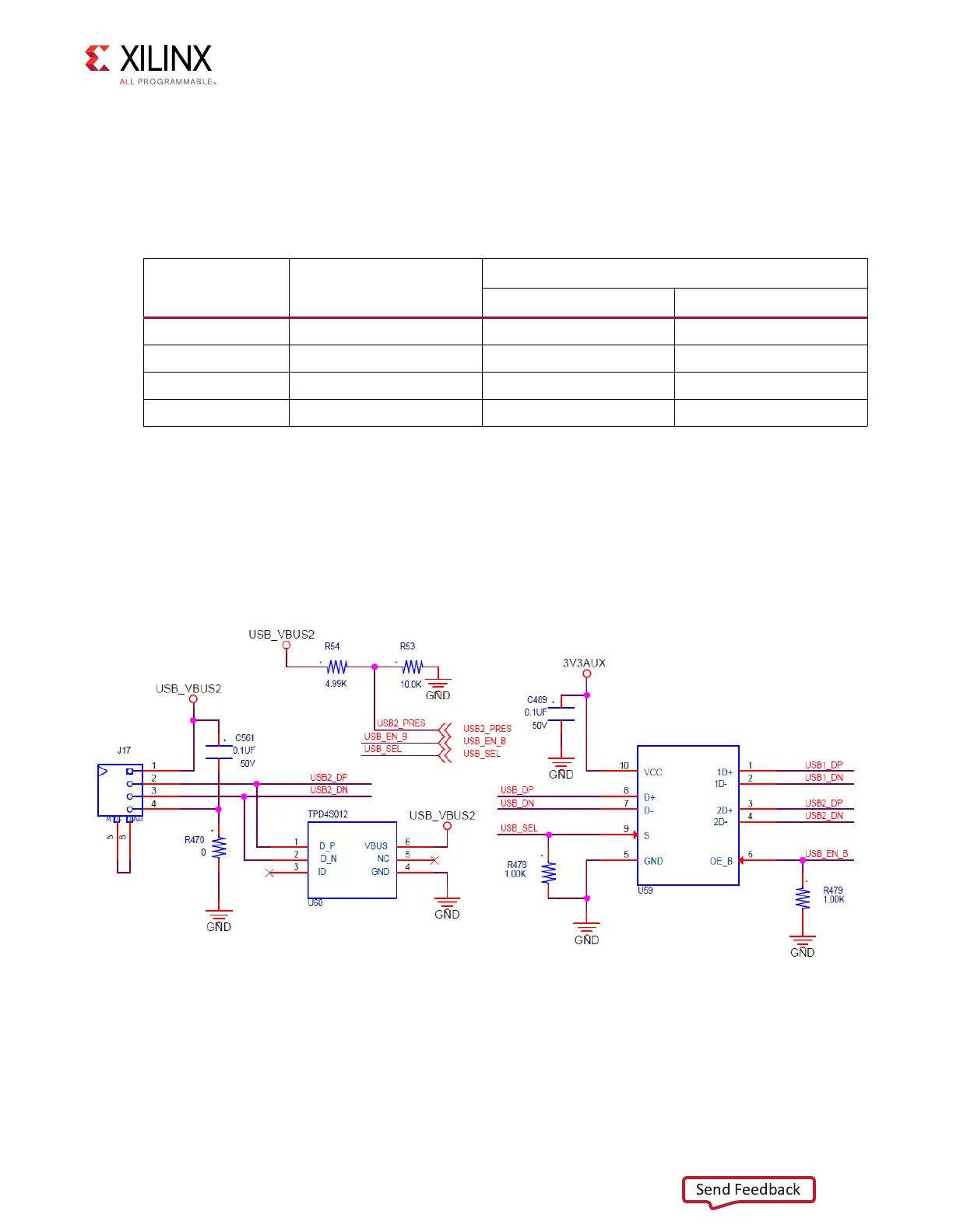
The VCU1525 revision D board implements a second USB connector. J17 is a keyed 1.2 mm
right-angle receptacle (Amphenol 10125839-04RAEHLF). J17 is selectable via TI
TS3USB221RSER 1-to-2 USB switch U59, which is controlled by the MSP432 U19 BMC. USB
switch U59 selects between the Micro-AB USB connector J13 (port 1) and the J17 4-pin
receptacle (port 2). J13 is selected by default at VCU1525 power on.
The USB switch circuit is shown in Figure 3-5.
Table 3-2: VCU1525 USB Switch Circuit Connections
Target Pin Net Name
FT4232HQ U27
Pin Name Pin
U13.BB20 USB_UART_RX BDBUS1 39
U13.BF18 USB_UART_TX BDBUS0 38
U19.7 FT2232H_UART_RX ACBUS1 27
U19.6 FT2232H_UART_TX ACBUS0 26
X-Ref Target - Figure 3-5
Figure 3-5: USB-UART Interface