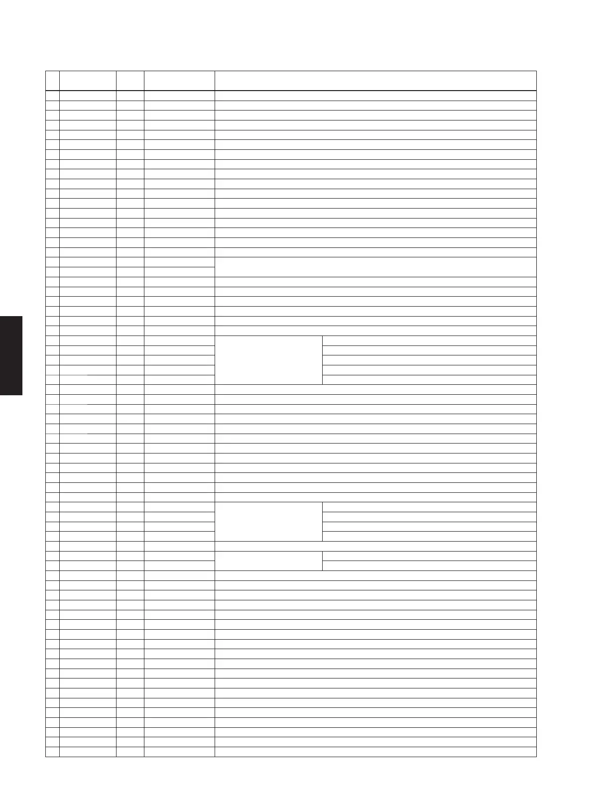
26
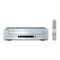
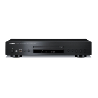
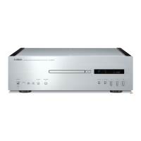
CD-C600
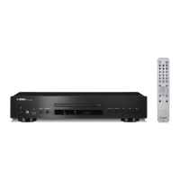
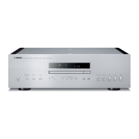
CD-C600
Pin
No.
Function
Name
I/O State During a Reset Detail of Function
1 EFMlN Al Input RF signal input
2 RFOUT AO Undefined RF signal output
3 LPF AO Undefined RF signal DC level detection low-pass filter capacitor connection
4 PHLPF AO Undefined Defect detection low-pass filter capacitor connection
5 AIN AI Input A signal input
6 CIN Al Input C signal input
7 BIN AI Input B signal input
8 DIN AI Input D signal input
9 SLCISET AI Input SLCO output current setting resistor connection
10 RFMON AO Undefined IC internal analog signal monitor
11 VREF AO AVDD/2 VREF voltage output
12 JITTC AO Undefined Jitter detection capacitor connection
13 EIN AI Input E signal input
14 FIN AI Input F signal input
15 PCNCNT AI Input EFM PLL charge pump control voltage input
16 TE AO Undefined TE signal output
17 TEIN AI Input TE signal input used for TES signal generation
18 LDD AO Undefined Laser power control signal output
Laser power detection signal input
19 LDS AI Input
20 AVSS — — Analog system ground / This pin must be connected to the 0 V level
21 AVDD — — Analog system power supply
22 FDO AO AVDD/2 Focus control signal output / D/A converter output
23 TDO AO AVDD/2 Tracking control signal output / D/A converter output
24 SLDO AO AVDD/2 Sled control signal output / D/A converter output
25 SPDO AO AVDD/2 Spindle control signal output / D/A converter output
26 VVSS1 — —
For use by the EFM PLL circuit
Internal VCO ground / This pin must be connected to the 0 V level
27 PDOUT1 O Undefined Internal VCO control phase comparator output 1
28 PDOUT0 O Undefined Internal VCO control phase comparator output 0
29 PCKIST AI Input PDOUT0, 1 output current setting resistor connection pin
30 VVDD1 — — Internal VCO power supply
31 CONT5 O Low General purpose output
32 CONT3 I/O Input General purpose input/output (Built-in pull-up resistor)
33 DEFECT I/O Input Monitor output pin (Defect detection signal output : High-active)
34 FSEQ I/O Input Monitor output pin (CD sync. signal detection output : High-active)
35 C2F I/O Input Monitor output pin (C2 error signal output : High-active)
36 DVDD — — Digital system power supply
37 DVSS — — Digital system ground / This pin must be connected to the 0 V level
38 DVDD15 AO High Digital circuit power supply capacitor connection
39 VVDD3 — — Internal PLL power supply
40 VVSS3 — — Internal PLL ground / This pin must be connected to the 0 V level
41 DVDD — — Digital system power supply
42 DVSS — — Digital system ground / This pin must be connected to the 0 V level
43 CE I Input
Host microprocessor interface
Host I/F : Chip enable signal input
44 CL I Input Host I/F : Data transfer clock input
45 DI I Input Host I/F : Data input
46 DO O Hi-Z (H) Host I/F : Data output (Trial-state output)
47 RESB I — IC reset input / This pin must be set low once after power is first applied
48 REG_READY0 O Low
Host microprocessor interface
Host I/F : REG_READY output (Nch-opendrain output)
49 SUB_READY0 O Low Host I/F : SUB_READY output (Nch-opendrain output)
50 CONT2 I/O Input General purpose input/output
51 CONT1 I/O Input General purpose input/output
52 CONT0 I/O Input General purpose input/output
53 MODE I — Set input / This pin must be connected to the DVDD
54 STREQ I/O Input Stream data demand signal output
55 STCK I/O Input Stream data bit clock input
56 STDATA I/O Input Stream data input
57 TEST I — Test input / This pin must be connected to the 0 V level
58 DATA I/O Input Monitor pin / Audio data output
59 DATACK I/O Input Monitor pin / Audio bit clock output
60 LRSY I/O Input Monitor pin / Audio Left/Right channel clock output
61 DVDD — — Digital system power supply
62 PCMLRSY O Low Monitor pin / Audio Left/Right channel clock output
63 PCMBCK O Low Monitor pin / Audio data shift clock output
64 PCMDATA O Low Monitor pin / Audio data serial output
65 PCMREQ I Input Monitor pin / Audio data output request signal input
66 DVDD15 AO High Digital circuit power supply capacitor connection
67 DVSS — — Digital system ground / This pin must be connected to the 0 V level
68 DVDD — — Digital system power supply