A
1
2
3
4
5
6
7
8
9
10
BCDEFGH I JK
L MN
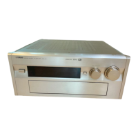
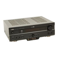
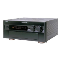
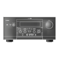
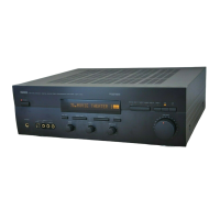
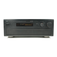
RX-V557/HTR-5850/DSP-AX557/RX-V457/HTR-5840/DSP-AX457
84
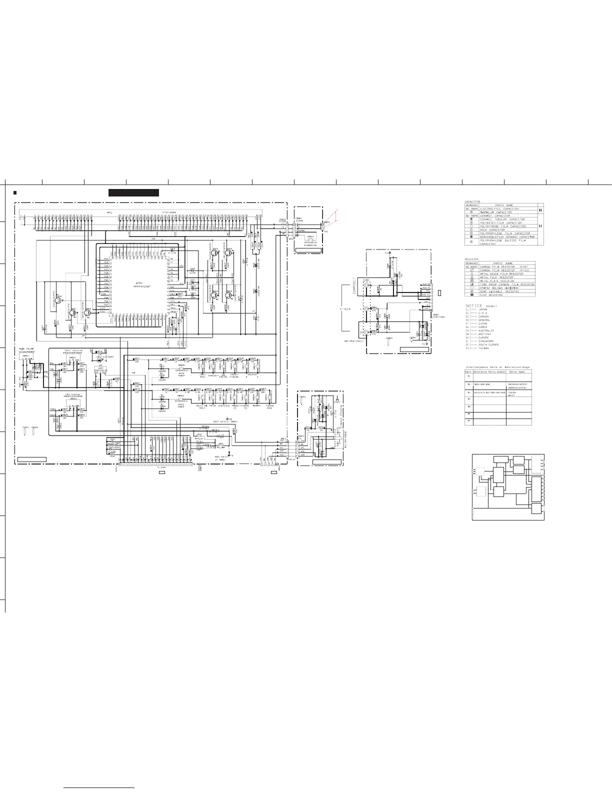
SCHEMATIC DIAGRAM (OPERATION) RX-V557/DSP-AX557
★ All voltages are measured with a 10MΩ/V DC electronic volt meter.
★ Components having special characteristics are marked s and must be replaced
with parts having specifications equal to those originally installed.
★ Schematic diagram is subject to change without notice.
★電圧は、内部抵抗10MΩの電圧計で測定したものです。
★
s印のある部品は、安全性確保部品を示しています。部品の交換が必要な場合、パーツリス
トに記載されている部品を使用してください。
★本回路図は標準回路図です。改良のため予告なく変更することがございます。
52
Display
controller
Segment
digit
select/
output
circuit
Serial
receive
circuit
Digit
output
circuit
Clock
generator
G12
51
G13
50
G14
49
48
47
P38
46
P37
45
P36
XOUT
6
VDD
8
Vcc2
18
Vss
5
Vp
64
XIN
7
3
4
/RESET
1
P35
44
9
P1
P9
17
19
P10
Segment
output
circuit
Display code
RAM
(8-bit x 60)
CGROM
(35 bit x 166)
CGROM
(35 bit x 16)
code
select
Code
write
Code/
command
control
circuit
G1
63
53
G11
IC801: M66003-0101FP
FL Display Driver
2
data
timing
clock
dot data
write
scan pulse
/CEFL
CKFL
DTFL
-21.0
-28.1
-22.5
-24.2
-26.2
-24.3
-18.9
-26.2
-26.2
-26.3
-26.3
-26.3
-26.3
-26.3
-26.3
-26.3
-24.4
-21.0
-26.3
-26.3
-26.3
-26.3
-26.3
-26.3
-26.3
-26.3
-26.3
-26.3
-26.3
-26.3
-26.3
-26.3
-26.2
-26.2
-26.2
-18.9
-26.3
-24.3
-22.5
-20.7
-26.3
-24.0
-26.2
-20.7
-24.3
-20.7
-22.6
-22.6
-21.0
-21.0
-20.7
-24.4
-17.1
-24.4
-26.2
-24.3
-28.1
-20.7
-28.3
-20.7
-24.4
-22.5
-22.6
-22.6
-26.2
-28.1
-26.3
-18.8
-20.7
-18.9
-24.3
-24.4
-17.0
-28.1
-20.7
-26.3
4.8
-17.1
-22.4
-20.7
-20.7
-22.6
-20.7
-28.1
-22.6
-22.5
-20.7
-22.5
-26.2
-26.3
-26.3
-26.3
-26.3
-26.3
-26.3
-26.3
-28.4
-26.2
-26.2 4.8
-24.4
-24.3
-20.7
-18.9
-26.3
-18.9
-17.0
-26.2
-26.2 4.8
-26.2
-26.2 4.8
-26.2
-28.1
-24.4
-24.4
-26.3
-22.6
-22.6
4.8
4.8
4.8
-24.4
-26.1
4.8
2.1
0
2.1
4.8
-20.7
-26.2 4.8
-26.1
-24.0 4.8
-24.9 -21.4-28.3 -24.9
-24.4
-22.3 4.8
-22.5
-18.8 4.8
-18.9
00
00
4.7 0
00
00
4.9
0
4.9
AC5.6
to FUNCTION
Page 83
G1
to FUNCTION
Page 83
J3
to SUBTR (2)
Page 88 H9
to POWER
TRANSFORMER
OPERATION (1)
OPERATION (3)
OPERATION (2)
OPERATION (4)
FL DRIVER
FL DISPLAY
 Loading...