•
SWL01U (YA876A01) CPU
DM: IC100
PIN
NO.
NAME I/O FUNCTION
PIN
NO.
NAME I/O FUNCTION
1 – – Unconnected inside 45 – – Unconnected inside
2 – – Unconnected inside 46 – – Unconnected inside
3
EA3/PD3/KYN24
I
ON/OFF signal from keyboard
47 – – Unconnected inside
4
EA2/PD2/KYN23
I 48 TXD0/PG4 O Serial port I/F
5
EA1/PD1/KYN22
I 49 RXDO/PH4 I Serial port I/F
6
EA0/PD0/KYN21
I 50 TXD1/PG2 O Serial port I/F
7
ED0/PC0/KYN11
I/O
Key selection signal to keyboard
51 RXD1/PH1 I Serial port I/F
8
ED1/PC1/KYN12
I/O 52 SCLK1/PH2 I Serial port I/F
9
ED2/PC2/KYN13
I/O 53 UCTL I
Fixed to L when USB is used /
Fixed to H when USB is unused
10
ED3/PC3/KYN14
I/O 54 VDD P Digital core power supply
11
ED4/PC4/KYN15
I/O 55 VSS G Digital core ground
12
ED5/PC5/KYN16
I/O 56 AVDD AP Analog poser supply
13
ED6/PC6/KYB05
I/O 57 AVREF AI ADC reference
14
ED7/PC7/KYB06
I/O 58 AN0 AI ADC input
15 PROTN I
For distinction between trial production and
commodity products
59 AN1 AI ADC input
16 BISTMD Is Memory BIST mode (1: BIST mode) 60 AN2 AI ADC input
17 BISTCLK Is Memory BIST clock 61 AN3 AI ADC input
18 PLLBPN Is PLL bypass mode (0: PLL bypass) 62 AGNDREF AI ADC ground reference
19 TESTN Is Test mode (0: test mode) 63 AVSS AG Analog ground
20 VSS G Digital core ground 64 USB VDD
USBP
USBIO power supply +1.8V
21 XI XI Crystal oscillator/Clock input (38.8688 MHz) 65 FUNC_DM IO USB data -
22 XO XO Crystal oscillator 66 FUNC_DP IO USB data +
23 VDD P Digital core power supply 67 USBVSS
USBG
USBIO ground
24 VSS G Digital core ground 68 USBIOVDD
USBIOP
USBIO power supply +3.3V
25 IOVDD IOP IO power supply 69 VSS G Digital core ground
26 TRSTN I JTAG I/F reset 70 VDD P Digital core power supply
27 TMS I JTAG I/F mode 71 XI_UCLK XI Crystal oscillator/Clock input (48 MHz)
28 TCK I JTAG I/F clock 72 XO_UCLK XO Crystal oscillator
29 TDI I JTAG I/F input 73 VSS G Digital core ground
30 TDO O JTAG I/F output 74 IOVDD IOP IO power supply
31 VDD P Digital core power supply 75 VBUS I USB Vbus
32 PLL VDD P
Digital PLL power supply (common to digital
core power supply inside)
76 PULLUPE O USB pull-up enable
33 PLL VSS G Digital core ground 77 CSON/PGO O Chip select for area 2
34 VSS G
Digital PLL ground (common to digital core
ground inside)
78 PDN/PF4 O External memory read signal
35 WCLK/SYO O Word clock (1Fs=44.1 kHz) 79 MA01 O External memory address
36 PFO O Port for output only 80 MD00 IO+
External memory data bus
37 SDO1 O Audio output data (with EQ & comp) 81 MD08 IO+
38 SDO0 O
(Output data equivalent to SWL01) /
Selection signal to keyboard
82 MD01 IO+
39 BCLK O Bit clock (64Fs) 83 MD09 IO+
40 SYSCLK/PG3 O System clock (256Fs/384Fs/768Fs) 84 MD02 IO+
41 SD1/PH3 I Serial audio input data 85 MD10 IO+
42 VSS G Digital core ground 86 – Unconnected inside
43 IRGON/PHO Is Interrupt input 87 – Unconnected inside
44 – – Unconnected inside 88 – Unconnected inside
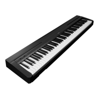
P-35B
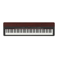
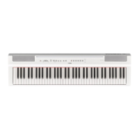
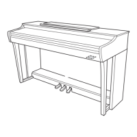
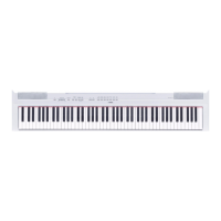
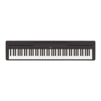
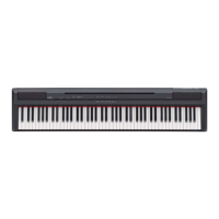
P-105B/P-105WH/P-35B/L-85WH/LP-5AWH
28
 Loading...