■
LSI PIN DESCRIPTION
(LSI 端子機能表)
CONTENTS
(目次)
• R8A02042BG (YC479A00) SWX08 ............................................26
• SWL01U (YA876A01) CPU ......................................................28
• μPD789022GB-A15-8E (XZ560100) CPU (MKS) ............................................30
• WM8524GEDT/R (YC681B00) DAC ......................30
• YDA175 (YD822A00) DIGITAL POWER AMPLIFIER ......................25
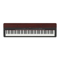
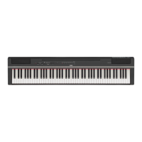
P-105B/P-105WH
P-105B/P-105WH
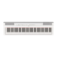
P-105B/P-105WH P-35B
P-105B/P-105WH P-35B
P-35B
•
YDA175 (YD822A00) DIGITAL POWER AMPLIFIER
DM: IC22 [P-105B/P-105WH], IC302 [P-35B]
P-105B/P-105WH P-35B
Note *1): I: Input pin, O: Output pin, A: Analog pin, O/D: Open-Drain output pin.
PVDD power pins should be connected each other on the boards. Likewise, GND pins should be also connected each other on it.
Each output pin with the same name (OUTPR, OUTMR, OUTPL and OUTML) should be connected on the board.
*2): A voltage for supplying SLEEP pin with H level should be applied from an external power supply. Do not apply from REFA pin output.
PIN
NO.
NAME I/O
*1)
FUNCTION
1 REFA AO Internal Regulator Output
2 AVSS GND Analog GND
3 N.C. – No Connection Pin. This pin must
be left open or connected to GND.
4 DVSS GND Digital GND
5 MCK I Master Clock Input Pin
6 SDATA I Audio Data Input Pin
7 SCLK I Bit Clock Input Pin
8 LRCLK I Word Clock Input Pin
9 PVDDPR PVDD power Power for the digital amplifier
output (Rch+)
10 OUTPR O Digital Amplifier Output (Rch+)
11 OUTPR O Digital Amplifier Output (Rch+)
12 PVSSR GND GND for the digital amplifier
output (Rch)
13 PVSSR GND GND for the digital amplifier
output (Rch)
14 OUTMR O Digital Amplifier Output (Rch-)
15 OUTMR O Digital Amplifier Output (Rch-)
16 PVDDMR PVDD power Power for the digital amplifier
output (Rch-)
17 SLEEPN I Sleep Reset pin
*2)
18 PROTN O/D Error Flag Output Pin
PIN
NO.
NAME I/O
*1)
FUNCTION
19 N.C. – No Connection Pin. This pin must
be left open or connected to GND.
20 N.C. – No Connection Pin. This pin must
be left open or connected to GND.
21 N.C. – No Connection Pin. This pin must
be left open or connected to GND.
22 CKMOD I Clock Mode Setting Pin
23 TEST – Test Pin. This pin must
be connected to GND.
24 MUTEN I Mute pin
25 PVDDML PVDD power Power for the digital amplifier
output (Lch-)
26 OUTML O Digital Amplifier Output (Lch-)
27 OUTML O Digital Amplifier Output (Lch-)
28 PVSSL GND GND for the digital amplifier output
(Lch)
29 PVSSL GND GND for the digital amplifier output
(Lch)
30 OUTPL O Digital Amplifier Output (Lch+)
31 OUTPL O Digital Amplifier Output (Lch+)
32 PVDDPL PVDD power Power for the digital amplifier
output (Lch+)
P-105B/P-105WH/P-35B/L-85WH/LP-5AWH
25
 Loading...