Do you have a question about the Yamaha P5000S and is the answer not in the manual?
| Power Output (8 ohms) | 500W |
|---|---|
| Power Output (8 ohms, Bridge) | 1500W |
| Frequency Response | 20Hz - 20kHz |
| Input Impedance | 20k ohms (balanced), 10k ohms (unbalanced) |
| Dimensions (W x H x D) | 480 x 88 x 456 mm |
| Total Harmonic Distortion | 0.1% |
| Connectors (Inputs) | XLR |
| Connectors (Outputs) | Speakon |
| Damping Factor | >300 (8 ohms, 1kHz) |
| Cooling System | Variable speed fan |
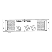
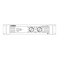
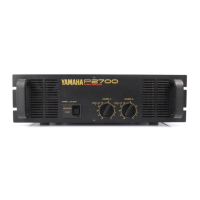
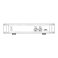
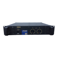
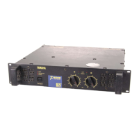
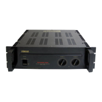
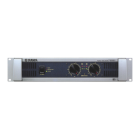
Identification and function of front panel switches, knobs, and indicators.
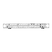
Identification and function of rear panel input, output, and control connectors.
Diagrams showing physical placement and wiring of main circuit boards.
Close-up views and specific wire routing details for internal connections.
Procedures for removing the rack angle and top cover.
Procedure for removing the Power Amplifier (PA) unit.
Procedures for removing PS, IN, OUT1, and OUT2 circuit boards.
Procedures for removing front panel, VR, Coil, LED, PSW boards, and handles.
Component layout and pattern diagram for the PAH circuit board.
Component layout and pattern diagram for the PS circuit board.
Component layout and pattern diagram for the IN circuit board.
Component layout and pattern diagram for the LED circuit board.
Component layout and pattern diagram for the OUT1 circuit board.
Component layout and pattern diagram for the OUT2 circuit board.
Component layout and pattern diagrams for PSW and VR circuit boards.
Component layout and pattern diagram for the COIL circuit board.
Setup for testing in STEREO/PARALLEL modes, including attenuator and load settings.
Checks for LEDs, fan, idle current, and output DC voltage.
Tests for gain, frequency response, distortion, noise, stability, and efficiency.
Setup and tests specifically for the BRIDGE mode of operation.
Table of PS board part numbers and corresponding line voltages.
Electrical performance requirements and capacitor discharge procedures for PS boards.
Detailed example of diagnosing and repairing a "no secondary output" fault.
Diagram of wiring for checks and final settings for product delivery.
Exploded view and parts list for chassis and external components.
Parts list and diagrams specific to the Power Amplifier (PA) unit components.
Detailed list of electronic components, including resistors, capacitors, transistors, and ICs.
External views and pin configurations for integrated circuits and diodes.
High-level block diagram showing signal flow and major functional units.
Detailed wiring diagram illustrating interconnections between various circuit boards.
Detailed circuit diagram for the input stage and signal processing.
Detailed circuit diagram for the Power Amplifier Heat-sink (PAH) section.
Continuation of the detailed circuit diagram for the PAH section.
Detailed circuit diagram for the Power Supply (PS) section.
Detailed circuit diagrams for LED, OUT, COIL, VR, and PSW sections.