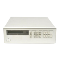
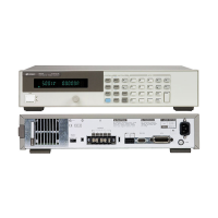
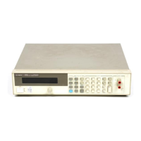
2-24 OUTPUT BOARD
The following paragraphs provide block diagram level
descriptions of the output board. The descriptions cover the
four output board types (40WLV, 40WHV, 8OWLV, and
80WHV). Differences between the board types are given as
required. Figure 2-1 shows which output board types are
used in each model.
The descriptions that follow are divided into two main
block diagram discussions: Secondary Interface Circuits and
Power Mesh and Control Circuits. The block diagrams
illustrate the major circuits and signal flow on an output
board. Complete circuit details are shown on the output
board functional schematic Figure 6-3 in the rear of the
manual. The functional names on the block diagrams
correspond with those on the functional schematic.
2-25 Secondary Interface Circuits (Figure 2-4)
and convert them to analog signals (voltages) which are sent
output voltage, output current, and overvoltage.
Measurement and status signals are sent back to the
secondary interface circuits from the power mesh and
control circuits to be processed before they are sent on to the
circuits shown in Figure 2-4.
2-26 Microcomputer. This 8-bit microcomputer (U312)
contains a CPU, ROM, and RAM. These internal circuits
and the power mesh and control circuits on the output
isolators which connect incoming data to an input port on
the microcomputer and outgoing data to an output port on
the microcomputer.
On the output board side, the microcomputer uses an 8-bit
parallel bidirectional data bus to program DACs which
control the output voltage, output current, and overvoltage
setting. Various status and operating conditions are read
back on the data bus. The microcomputer also generates
address and control signals which are used by other
interface circuits. The interrupt input to the microcomputer
is used in conjunction with analog multiplexer (U323) and
DAC (U321) to perform a succesive approximation A/D
conversion in order to readback output voltage and current
values as well as various test point voltages.
2-27 Address Decoder. This circuit (U320) decodes
addresses sent by the microcomputer and generates the
appropriate chip select signal (CS0 - CS3) to select which
circuit sends or receives data. CS0 selects the status monitor
(part of U327) to send status data back to the
microcomputer on data bus lines D0-D5. CS1-CS3 determine
which DAC will receive data. CS1 selects the CV 12-bit
DAC, CS2 selects the + CC/OV dual 8-bit DAC, and CS3
selects the readback 12-bit DAC.
2-28 CV DAC. The constant voltage (CV) 12-bit DAC
(U313) and amplifier (U315A) convert the digital input into
an analog signal (CV REF) in the range of 0 to -10 V. This
signal is used as a reference voltage and is sent to the
voltage control circuits (see paragraph 2-43) to set the
output voltage to the programmed value. CV REF is also
sent to the analog multiplexer so that it can be measured
during power on self test.
The 12-bit DAC internally formulates the 12-bit DAC data
from the 8-bit (D0-D7) data bus. Bits D4-D7 are transferred
into DAC bit positions 0-3 when the microcomputer sets the
DAC A/B signal low and bits D0-D7 are transferred into
DAC bit positions 4-11 when the microcomputer sets the
DAC A/B signal high.
2-29 Current and Overvoltage DACs. These DACs are
contained in a dual 8-bit DAC chip (U314). The DAC A/B
signal determines which DAC receives the data on the data
bus. Bits D0-D7 are transferred into the current DAC when
DAC A/B is low and into the overvoltage DAC when DAC
A /B is high.
The 8-bit current DAC (part of U314) and amplifier U315B
convert the digital input into an analog signal (CL REF) in
the range of 0 to -10 V. This signal is used as a reference
voltage and is sent to the current control circuit (see
paragraph 2-44) to set the output current to the
programmed value.
The 8-bit overvoltage DAC (part of U314) and amplifier
U315C convert the digital input into an analog signal (OV
REF) in the range of 0 to -10 V. This signal is compared with
the output voltage and will shut down the output when the
output voltage exceeds the programmed OV (see paragraph
2-32).
The CL REF and OV REF signals are also sent to the analog
multiplexer so that they can be measured during power on
self test.
2-30 Analog Multiplexer. The analog multiplexer
(U323)selects one of eight inputs (0 to -10 V) to be applied to
the readback signal comparator for the A/D converter. The
selected signal is determined by address lines (A0-A2)
which are received from the microcomputer. The analog
inputs to the multiplexer indicate the following:
COM - hardwired to common to reduce noise
when no signals are being sampled.
FUSE - output board's return fuse status
(read back during power-on self test)
V READBACK - output voltage
-I READBACK - output current (sink)
- output current (source)
CV REF - voltage DAC output
CL REF - current DAC output
OV REF - overvoltage DAC output
2-7
__
__
__
__
__
___
___
___ ___
___
________
to the power mesh and control circuits to program the
+I READBACK
These circuits receive digital signals from the GPIB board
GPIB board and then to the GPIB controller and/or the front
panel. The following paragraphs describe the interface
process all data that is transferred between the GPIB board
board. GPIB board data is transferred serially via optical