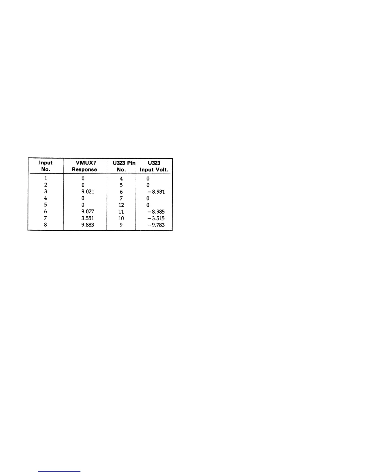
The next program uses a FOR/NEXT loop to read the 8
associated input nos. are printed by the computer (see Input
and Response columns in the table below).
10 FOR X=1 TO 8
20 OUT 705;”VMUX? 2";X
30 ENTER 705;V
40 PRINT X,V
50 NEXT X
60 END
The table below shows the 8 measured input voltage values
as well as the VMUX? response for a typical calibrated
40WLV output (no load connected) whose voltage and
current have been programmed to their High Range Full
Scalue values (20V and 2A) and the OV (overvoltage) to 23
V.
If all of the inputs read back by the VMUX? command are
circuitry (U321-U324) is probably defective. If only one
input is incorrect, the circuitry associated with that one
input is probably defective (see Figure 6-3).
4-30 Understanding and Troubleshooting the
Signal Processor U327
This custom IC processes both analog and digital signals to
interface the microcomputer (U312) with the power mesh
and control circuits. The signal processor circuits can be
functionally divided into three areas: overvoltage and
driver, power-on/start-up, and status monitor circuits. A
general description of this IC is provided in paragraph 2-32.
The following information will help you troubleshoot the
three signal processor functions.
Proper operation of the IC can be verified by measuring the
pin voltages and using Table 4-16 which lists the voltage
levels and defines the low and high states. This information
is used in conjunction with the pin descriptions (paragraph
4-31) and simplified schematics to troubleshoot the signal
processor's overvoltage (Figure 4-17), power-on/start-up
(Figure 4-18), and status monitor circuits (Figure 4-19).
Additional troubleshooting information for the status
monitor circuit is given in paragraph 4-32 and Figure 4-20.
4-31 Signal Processor (U327) Pin Function Descriptions.
The signal processor's circuits are shown on the functional
schematic of Figure 6-3, sheet 1, and on the block diagram of
Figure 2-4. The 28 signal processor pins are described as
follows:
+ 5 V (pin 1): The + 5 V bias voltage can range from 4.72 V
to 5.23 V.
OV COMP (pin 2): The OV COMP (overvoltage
comparator) input signal, when High, causes OV DRIVE
(pin 6) to be High (> 8 V) if POV DISABLE (pin 3) is Low.
POV DISABLE (pin 3): The POV DISABLE (programmed
overvoltage disable) input signal, when High, prevents OV
COMP (pin 2) from causing OV DRIVE (pin 6) to be High. It
does not prevent OV TRIP (pin 4) from causing OV Drive to
be High.
OV TRIP (pin 4): This input signal, when High, causes OV
DRIVE (pin 6) to be High (> 11 V) independent of POV
DISABLE (pin 3).
Common (pin 5): Along with pin 22, this is a common
return for the bias supplies.
OV DRIVE (pin 6): This output signal is a function of
inputs: OV COMP, POV DISABLE, and OV TRIP. When OV
DRIVE goes High, it fires the SCR in the power module. The
OV DRIVE pin voltage will be > 8 V when tripped from OV
COMP and > 11 V when tripped from OV TRIP (see Figure
4-17).
STATUS RESET (pin 7): This input pin, when High, causes
four internal flip-flops to be reset. The four flip-flops are
used to catch and hold the occurrence of four status
conditions: CV, + CC, - CC, and UNR.
+ 15 V (pin 8): The + 15 V bias voltage can range from 14 V
to 15.66 V.
UNREG (pin 9): The UNREG (unregulated) output signal
(open collector) takes on the state of the internal UNR flip-
flop when STATUS SELECT (pin 11) is Low. The
unregulated mode is indicated when UNREG is Low. Figure
4-19 shows the conditions that cause UNREG to go Low.
UNREG is open-circuited when STATUS SELECT is High.
- CLO (pin 10): The -CLO (-current limit output) output
signal (open collector) takes on the state of the internal -CC
flip-flop when STATUS SELECT (pin 11) is Low. The –CC
mode is indicated when -CLO is Low. Figure 4-19 shows the
conditons that cause -CLO to be Low. -CLO is open-
circuited when STATUS SELECT is High.
STATUS SELECT (pin 11): This input signal, when Low,
causes the four status conditions held in the flip-flops as
well as the overvoltage and overtemperature signals to be
transferred to the six output pins on the data bus (CVO,
+CLO, -CLO, UNREG, OV, and OT). When STATUS
SELECT is High, the six output pins are open-circuited.
4-50
________________
______________
_______
_______
_______
_______ _______
_______
_______
______________
______________
______________
_____ _____
_____
_____
_____
_____
_____ _____ ________
analog multiplexer inputs one at a time. The readings and
incorrect, the analog multiplexer U323 and/or the readback