Description
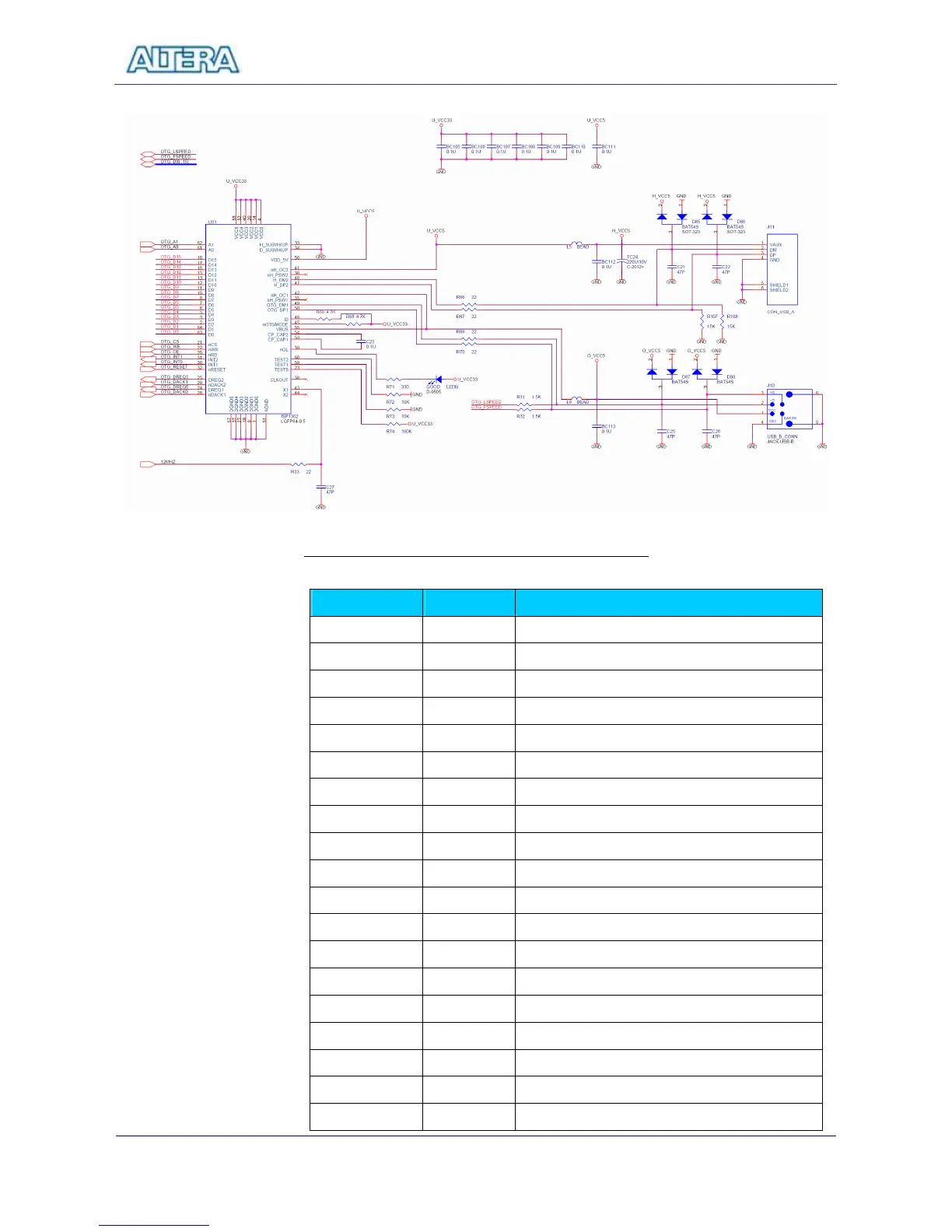
OTG_ADDR[0] PIN_K7 ISP1362 Address[0]
OTG_ADDR[1] PIN_F2 ISP1362 Address[1]
OTG_DATA[0] PIN_F4 ISP1362 Data[0]
OTG_DATA[1] PIN_D2 ISP1362 Data[1]
OTG_DATA[2] PIN_D1 ISP1362 Data[2]
OTG_DATA[3] PIN_F7 ISP1362 Data[3]
OTG_DATA[4] PIN_J5 ISP1362 Data[4]
OTG_DATA[5] PIN_J8 ISP1362 Data[5]
OTG_DATA[6] PIN_J7 ISP1362 Data[6]
OTG_DATA[7] PIN_H6 ISP1362 Data[7]
OTG_DATA[8] PIN_E2 ISP1362 Data[8]
OTG_DATA[9] PIN_E1 ISP1362 Data[9]
OTG_DATA[10] PIN_K6 ISP1362 Data[10]
OTG_DATA[11] PIN_K5 ISP1362 Data[11]
OTG_DATA[12] PIN_G4 ISP1362 Data[12]
OTG_DATA[13] PIN_G3 ISP1362 Data[13]
OTG_DATA[14] PIN_J6 ISP1362 Data[14]
OTG_DATA[15] PIN_K8 ISP1362 Data[15]
OTG_CS_N PIN_F1 ISP1362 Chip Select