Program images into On-chip CFM flash and external QSPI flash
The following steps describe how to program FPGA image into MAX 10 FPGA On-chip CFM
flash for internal configuration and software image(s) into on-board QSPI flash.
How to program the factory images into MAX 10 FPGA device and Quad SPI flash:
1. Program *\software_examples\factory_images\dual_boot_image.pof into Configuration
Flash Memory (CFMs) via programmer
2. Change SW2 switch 2 to the ON position (0)
3. Make sure Ethernet cable is connected to port A (the bottom one)
4. Power cycle the board or push S5 button to boot up from BUP build (BUP A)
5. Open NIOS command shell at *\altera\15.0\nios2eds\, e.g. double click "Nios II Command
Shell.bat"
6. Change directory to *\software_examples\factory_images\
7. Type "nios2-download --cable n* --device 1 -g -r ./web_server.elf; nios2-terminal;"
8. Check whether it gets corresponding IP address
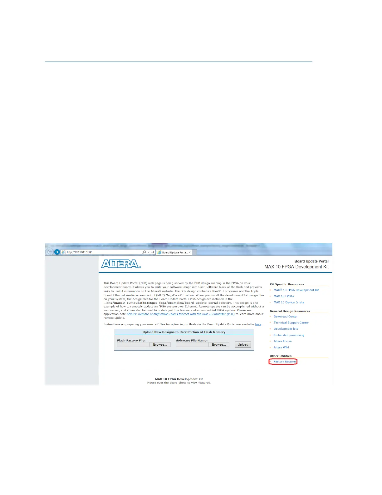
9. Launch IE and type the IP address got from step #g in the address bar (e.g.
http://192.168.1.100, Change Proxy Server setting if needed)
10. If it turns out be the MAX 10 FPGA development kit Webpage, please click the bottom-right
"Factory Restore" link to restore factory build, otherwise, it should be the raw page for
factory build programming
Figure 8: MAX 10 FPGA development kit Webpage