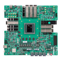
GTM214/215/216/217: OSFP
[Figure 3, callout 55]
The ACAP (U1) banks 214/215/216/217 GTM transceivers are wired to the QSFPDD6
connector J362. The connector is TE connecvity connector 2344064-4, rated at 112 Gb/s per
lane.
The transceivers are wired in an opmized paern to be operated at 112 Gb/s per lane. This
conguraon was chosen to provide 800GAUI-8 funconality.
For connecvity details, see the table in the Transceivers secon and schemac page 60. See the
Versal ACAP GTM Transceivers Architecture Manual (AM017) for more details on GTM-Quad
conguraons.
GTM219: SMA/1588 PPS
[Figure 3, callout 41]
The ACAP (U1) bank 219 GTM transceivers are wired to the SMA connectors J373, J374, J375,
and J376. The connectors are the Carlisle SMA TMB-V5F2-3L1, rated at 34 GHz. The remainder
of the ACAP (U1) bank 219 GTM transceivers are wired to the Renesas 8A34001 system
synchronizer (U219). This provides for an IEEE 1588 PPS signal. This is intended to be coupled
with REFCLK0, which has been ed to an output from the Renesas 8A34001 (U219) system
synchronizer for IEEE 1588 use.
The transceivers are wired in an opmized paern to be operated at 112 Gb/s per lane. This
conguraon was chosen to provide exibility for evaluaon of GTM transceivers.
For connecvity details, see the table in the Transceivers secon and schemac page 18. See the
Versal ACAP GTM Transceivers Architecture Manual (AM017) for more details on GTM-Quad
conguraons.
QSFP-DD Control Signals
The QSFP-DD control signals can be asserted in mulple ways. Each QSFP-DD has an I2C
connecon to the I2C1 bus through the I2C mulplexer (TCA9548PWR U35) as shown in the
PMC MIO[44:45] I2C1 Bus secon.
The following table lists the transceiver module control signals.
Table 18:
Transceiver Module Control Signals
Signal Name Feature Notes
Schematic
Page
QSFPDD_I2C_SDA Two-wire interface data U35 I2C MUX 56-59
QSFPDD_I2C_SCL Two-wire interface clock U35 I2C MUX 56-59
Chapter 3: Board Component Descriptions
UG1582 (v1.0) February 21, 2023 www.xilinx.com
VPK180 Board User Guide 59