AT90S4414/8515
9
ALU - Arithmetic Logic Unit
The high-performance AVR ALU operates in direct connection with all the 32 general purpose working registers. Within a
single clock cycle, ALU operations between registers in the register file are executed. The ALU operations are divided into
three main categories - arithmetic, logical and bit-functions.
In-System Programmable Flash Program Memory
The AT90S4414/8515 contains 4K/8K bytes on-chip In-System Programmable Flash memory for program storage. Since
all instructions are 16-or 32-bit words, the Flash is organized as 2K x 16/4K x 16. The Flash memory has an endurance of
at least 1000 write/erase cycles. The AT90S4414/8515 Program Counter (PC) is 11/12 bits wide, thus addressing the
2048/4096 program memory addresses.
See page 77 for a detailed description on Flash data downloading.
See page 10 for the different program memory addressing modes.
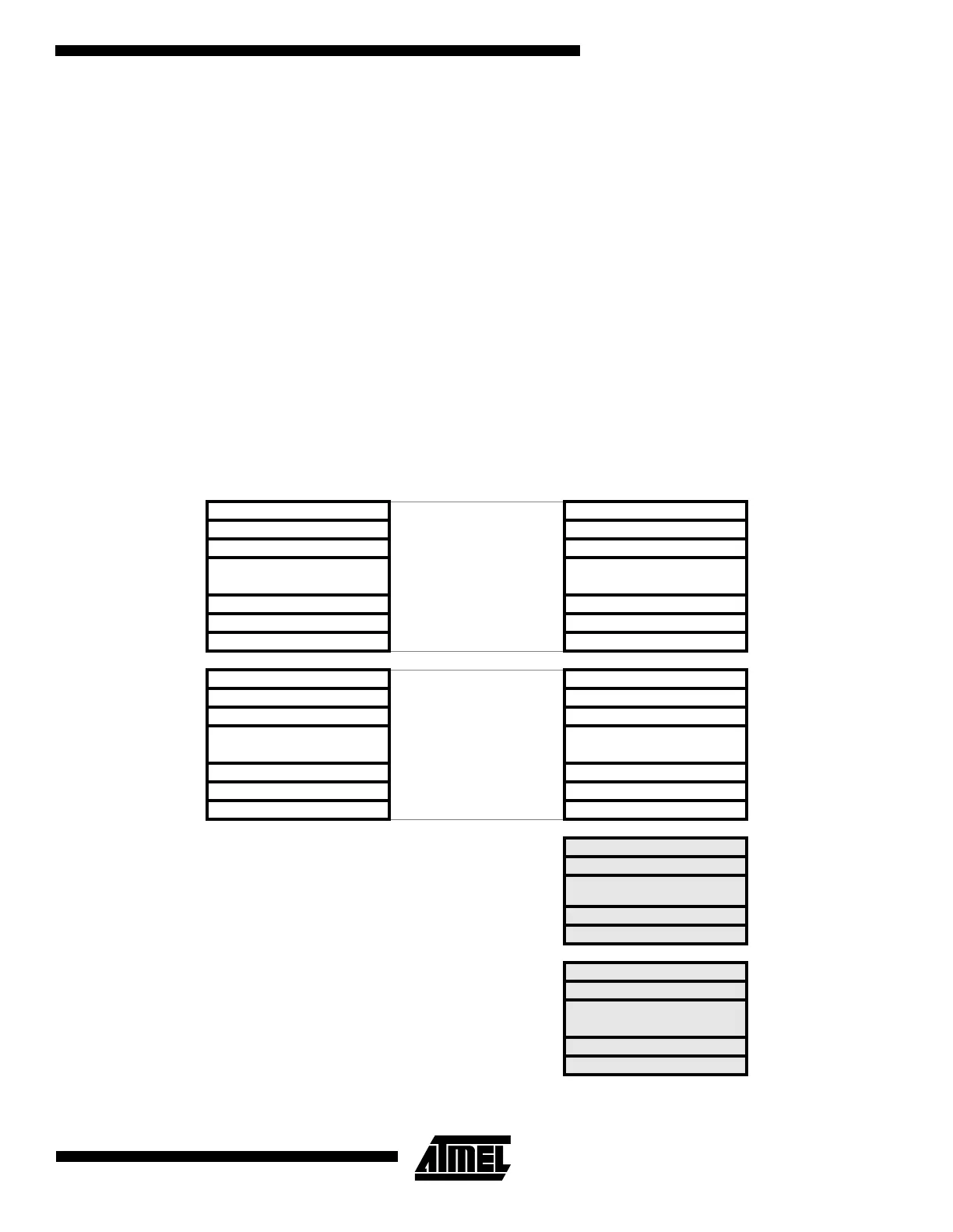
SRAM Data Memory - Internal and External
The following figure shows how the AT90S4414/8515 SRAM Memory is organized:
Figure 8. SRAM Organization
Register File Data Address Space
R0 $0000
R1 $0001
R2 $0002
……
R29 $001D
R30 $001E
R31 $001F
I/O Registers
$00 $0020
$01 $0021
$02 $0022
……
$3D $005D
$3E $005E
$3F $005F
Internal SRAM
$0060
$0061
…
$015E/$025E
$015F/$025F
External SRAM
$0160/$0260
$0161/$0261
…
$FFFE
$FFFF

 Loading...


