AT90S4414/8515
83
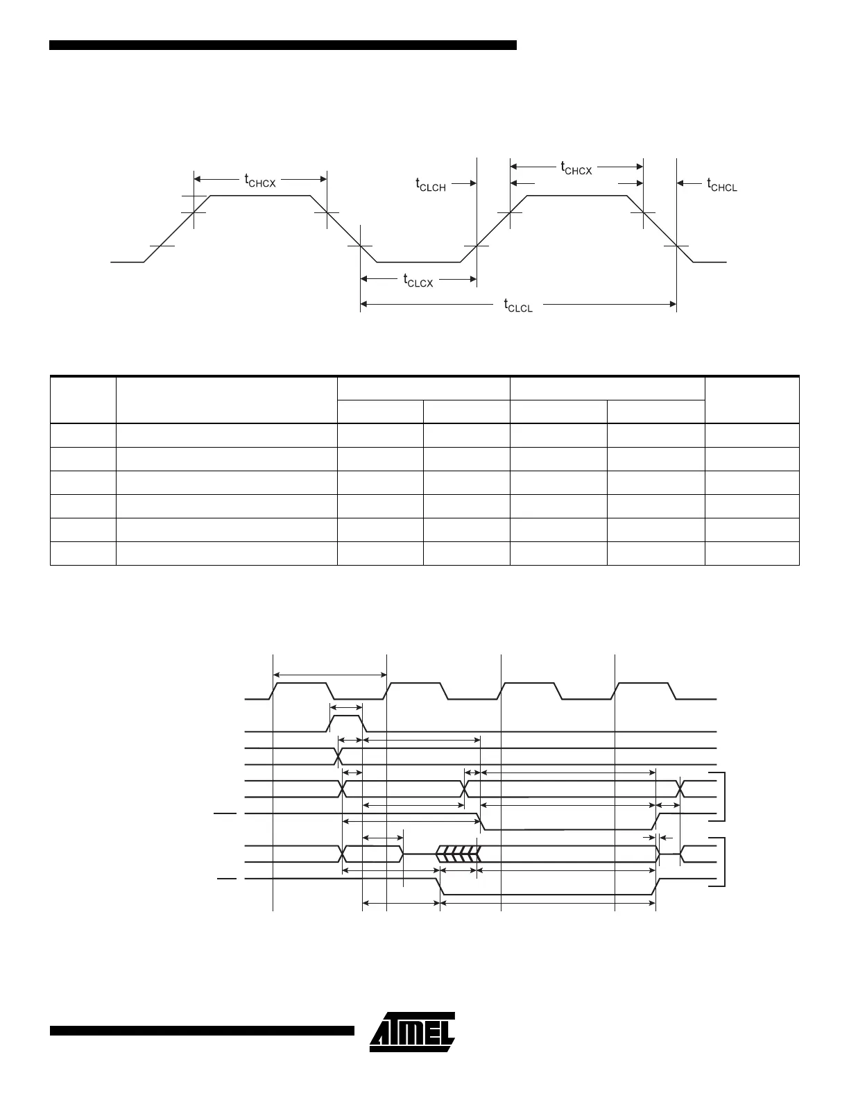
External Clock Drive Waveforms
Figure 67. External Clock
Note: See “External Data Memory Timing” on page 84. for a description of how the duty cycle influences the timing for the External
Data Memory
Figure 68. External RAM Timing
T3 is only present when wait-state is enabled.
Table 37. External Clock Drive
Symbol Parameter
V
CC
= 2.7V to 4.0V V
CC
= 4.0V to 6.0V
UnitsMin Max Min Max
1/t
CLCL
Oscillator Frequency 0 4 0 8 MHz
t
CLCL
Clock Period 250 125 ns
t
CHCX
High Time 100 50 ns
t
CLCX
Low Time 100 50 ns
t
CLCH
Rise Time 1.6 0.5 µs
t
CHCL
Fall Time 1.6 0.5 µs
VIL1
VIH1
System Clock O
ALE
WR
RD
Data / Address [7..0]
Data / Address [7..0]
Address [15..8]
Address
Address
Address
T1 T2 T3 T4
Prev. Address
Prev. Address
Prev. Address
1
0
4
213
3a
5
Note: Clock cycle T3 is only present when external SRAM waitstate is enabled
10
12
14
15
11
8
9
16
7
6
3b
Data
Data
WriteRead
Addr.
Addr.

 Loading...


