AT90S4414/8515
96
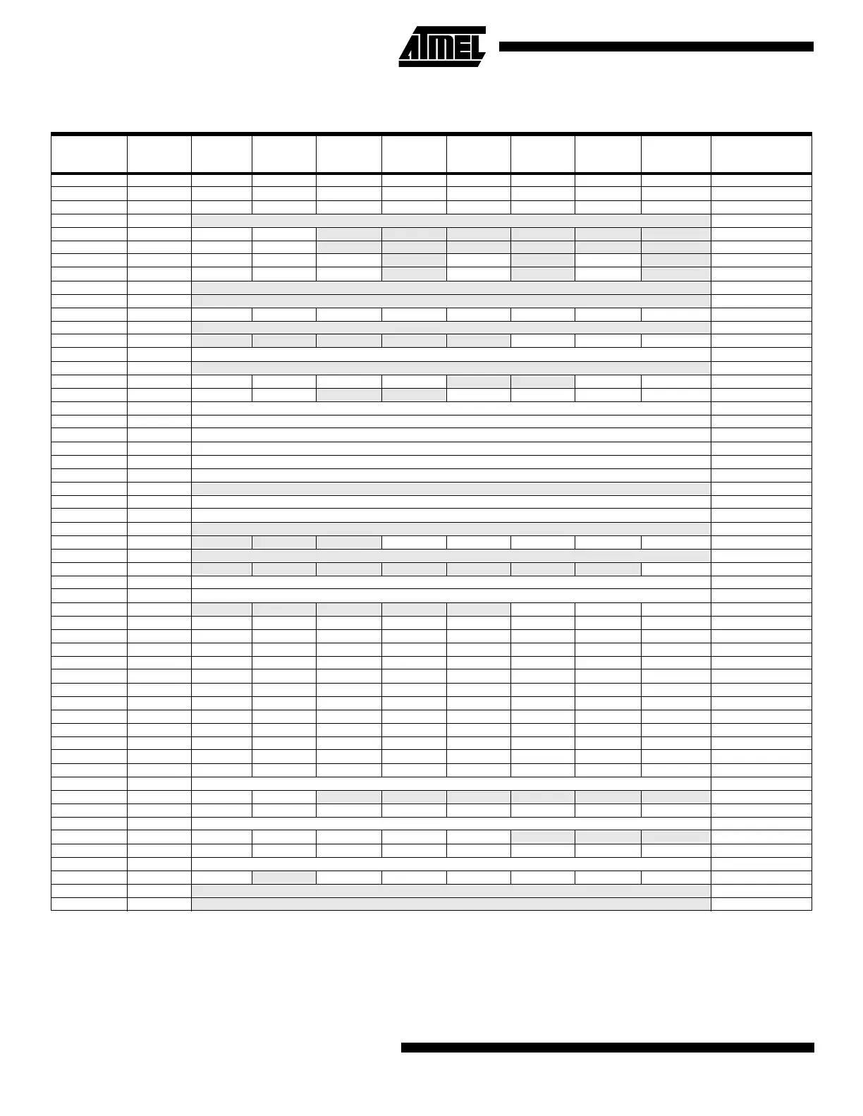
Notes: 1. EEARH only present for AT90S8515
2. For compatibility with future devices, reserved bits should be written to zero if accessed. Reserved I/O memory addresses
should never be written.
3. Some of the status flags are cleared by writing a logical one to them. Note that the CBI and SBI instructions will operate on
all bits in the I/O register, writing a one back into any flag read as set, thus clearing the flag. The CBI and SBI instructions
work with registers $00 to $1F only.
Register Summary
Address Name Bit 7 Bit 6 Bit 5 Bit 4 Bit 3 Bit 2 Bit 1 Bit 0 Page
$3F ($5F) SREG I T H S V N Z C 18
$3E ($5E) SPH SP15 SP14 SP13 SP12 SP11 SP10 SP9 SP8 19
$3D ($5D) SPL SP7 SP6 SP5 SP4 SP3 SP2 SP1 SP0 19
$3C ($5C) Reserved
$3B ($5B) GIMSK INT1 INT0 - - - - - -24
$3A ($5A) GIFR INTF1 INTF0
24
$39 ($59) TIMSK TOIE1 OCIE1A OCIE1B
- TICIE1 - TOIE0 -25
$38 ($58) TIFR TOV1 OCF1A OCF1B
-ICF1-TOV0 -25
$37 ($57) Reserved
$36 ($56) Reserved
$35 ($55) MCUCR SRE SRW SE SM ISC11 ISC10 ISC01 ISC00 27
$34 ($54) Reserved
$33 ($53) TCCR0 - - - - - CS02 CS01 CS00 30
$32 ($52) TCNT0 Timer/Counter0 (8 Bit) 31
... Reserved
$2F ($4F) TCCR1A COM1A1 COM1A0 COM1B1 COM1B0 - -PWM11PWM10 32
$2E ($4E) TCCR1B ICNC1 ICES1
- - CTC1 CS12 CS11 CS10 33
$2D ($4D) TCNT1H Timer/Counter1 - Counter Register High Byte 34
$2C ($4C) TCNT1L Timer/Counter1 - Counter Register Low Byte 34
$2B ($4B) OCR1AH Timer/Counter1 - Output Compare Register A High Byte 35
$2A ($4A) OCR1AL Timer/Counter1 - Output Compare Register A Low Byte 35
$29 ($49) OCR1BH Timer/Counter1 - Output Compare Register B High Byte 35
$28 ($48) OCR1BL Timer/Counter1 - Output Compare Register B Low Byte 35
... Reserved
$25 ($45) ICR1H Timer/Counter1 - Input Capture Register High Byte 36
$24 ($44) ICR1L Timer/Counter1 - Input Capture Register Low Byte 36
... Reserved
$21 ($41) WDTCR - - - WDTOE WDE WDP2 WDP1 WDP0 38
$20 ($40) Reserved
$1F ($3F) EEARH
1
- - - - - - - EEAR8 39
$1E ($3E) EEARL EEPROM Address Register Low Byte 39
$1D ($3D) EEDR EEPROM Data Register 40
$1C ($3C) EECR
- - - - - EEMWE EEWE EERE 40
$1B ($3B) PORTA PORTA7 PORTA6 PORTA5 PORTA4 PORTA3 PORTA2 PORTA1 PORTA0 55
$1A ($3A) DDRA DDA7 DDA6 DDA5 DDA4 DDA3 DDA2 DDA1 DDA0 55
$19 ($39) PINA PINA7 PINA6 PINA5 PINA4 PINA3 PINA2 PINA1 PINA0 55
$18 ($38) PORTB PORTB7 PORTB6 PORTB5 PORTB4 PORTB3 PORTB2 PORTB1 PORTB0 57
$17 ($37) DDRB DDB7 DDB6 DDB5 DDB4 DDB3 DDB2 DDB1 DDB0 57
$16 ($36) PINB PINB7 PINB6 PINB5 PINB4 PINB3 PINB2 PINB1 PINB0 57
$15 ($35) PORTC PORTC7 PORTC6 PORTC5 PORTC4 PORTC3 PORTC2 PORTC1 PORTC0 62
$14 ($34) DDRC DDC7 DDC6 DDC5 DDC4 DDC3 DDC2 DDC1 DDC0 62
$13 ($33) PINC PINC7 PINC6 PINC5 PINC4 PINC3 PINC2 PINC1 PINC0 62
$12 ($32) PORTD PORTD7 PORTD6 PORTD5 PORTD4 PORTD3 PORTD2 PORTD1 PORTD0 64
$11 ($31) DDRD DDD7 DDD6 DDD5 DDD4 DDD3 DDD2 DDD1 DDD0 64
$10 ($30) PIND PIND7 PIND6 PIND5 PIND4 PIND3 PIND2 PIND1 PIND0 64
$0F ($2F) SPDR SPI Data Register 45
$0E ($2E) SPSR SPIF WCOL
- - - - - -45
$0D ($2D) SPCR SPIE SPE DORD MSTR CPOL CPHA SPR1 SPR0 44
$0C ($2C) UDR UART I/O Data Register 48
$0B ($2B) USR RXC TXC UDRE FE OR
- - -49
$0A ($2A) UCR RXCIE TXCIE UDRIE RXEN TXEN CHR9 RXB8 TXB8 49
$09 ($29) UBRR UART Baud Rate Register 51
$08 ($28) ACSR ACD
- ACO ACI ACIE ACIC ACIS1 ACIS0 52
… Reserved
$00 ($20) Reserved

 Loading...


