AT90S4414/8515
30
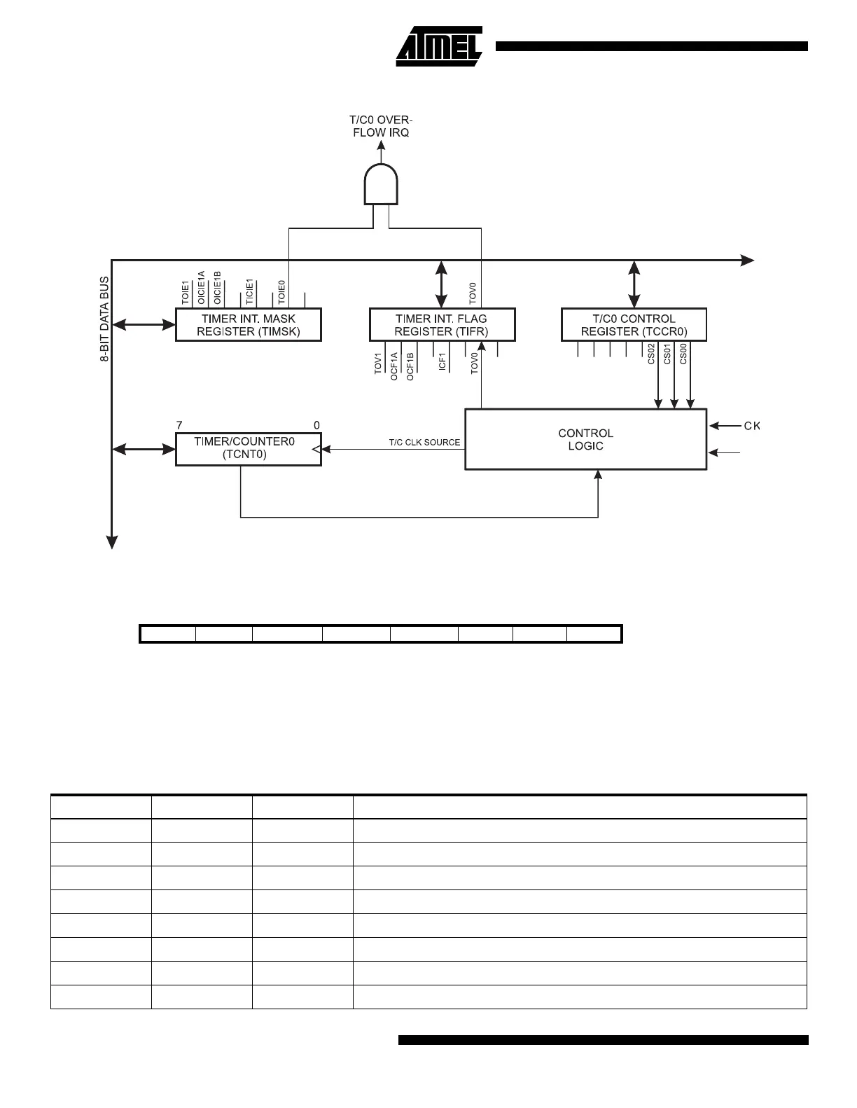
Figure 29. Timer/Counter0 Block Diagram
Timer/Counter0 Control Register - TCCR0
•
Bits 7..3 - Res: Reserved bits
These bits are reserved bits in the AT90S4414/8515 and always read as zero.
•
Bits 2,1,0 - CS02, CS01, CS00: Clock Select0, bit 2,1 and 0
The Clock Select0 bits 2,1 and 0 define the prescaling source of Timer/Counter0.
Bit 7 6 5 4 3 2 1 0
$33 ($53) - - - - - CS02 CS01 CS00 TCCR0
Read/Write R R R R R R/W R/W R/W
Initial value 0 0 0 0 0 0 0 0
Table 8. Clock 0 Prescale Select
CS02 CS01 CS00 Description
0 0 0 Stop, the Timer/Counter0 is stopped.
001CK
010CK/8
011CK/64
100CK/256
101CK/1024
1 1 0 External Pin T0, falling edge
1 1 1 External Pin T0, rising edge
T0

 Loading...


