AT90S4414/8515
36
Timer/Counter1 Input Capture Register - ICR1H AND ICR1L
The input capture register is a 16-bit read-only register.
When the rising or falling edge (according to the input capture edge setting - ICES1) of the signal at the input capture pin -
ICP - is detected, the current value of the Timer/Counter1 is transferred to the Input Capture Register - ICR1. At the same
time, the input capture flag - ICF1 - is set (one).
Since the Input Capture Register - ICR1 - is a 16-bit register, a temporary register TEMP is used when ICR1 is read to
ensure that both bytes are read simultaneously. When the CPU reads the low byte ICR1L, the data is sent to the CPU and
the data of the high byte ICR1H is placed in the TEMP register. When the CPU reads the data in the high byte ICR1H, the
CPU receives the data in the TEMP register. Consequently, the low byte ICR1L must be accessed first for a full 16-bit
register read operation.
The TEMP register is also used when accessing TCNT1, OCR1A and OCR1B. If the main program and also interrupt
routines perform access to registers using TEMP, interrupts must be disabled during access from the main program (and
from interrupt routines if interrupts are allowed from within interrupt routines).
Timer/Counter1 In PWM Mode
When the PWM mode is selected, Timer/Counter1 and the Output Compare Register1A - OCR1A and the Output Compare
Register1B - OCR1B, form a dual 8, 9 or 10-bit, free-running, glitch-free and phase correct PWM with outputs on the
PD5(OC1A) and OC1B pins. Timer/Counter1 acts as an up/down counter, counting up from $0000 to TOP (see Table 12),
where it turns and counts down again to zero before the cycle is repeated. When the counter value matches the contents of
the 10 least significant bits of OCR1A or OCR1B, the PD5(OC1A)/OC1B pins are set or cleared according to the settings of
the COM1A1/COM1A0 or COM1B1/COM1B0 bits in the Timer/Counter1 Control Register TCCR1A. Refer to Table 13 for
details.
Note: X = A or B
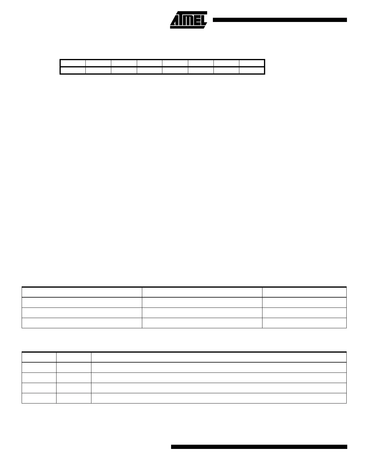
Bit 151413121110 9 8
$25 ($45) MSB ICR1H
$24 ($44) LSB ICR1L
76543210
Read/Write RRRRRRRR
RRRRRRRR
Initial value 0 0 0 0 0 0 0 0
00000000
Table 12. Timer TOP Values and PWM Frequency
PWM Resolution Timer TOP value Frequency
8-bit $00FF (255) f
TCK1
/510
9-bit $01FF (511) f
TCK1
/1022
10-bit $03FF(1023) f
TCK1
/2046
Table 13. Compare1 Mode Select in PWM Mode
COM1X1 COM1X0 Effect on OCX1
0 0 Not connected
0 1 Not connected
1 0 Cleared on compare match, up-counting. Set on compare match, down-counting (non-inverted PWM).
1 1 Cleared on compare match, down-counting. Set on compare match, up-counting (inverted PWM).

 Loading...


