EasyManua.ls Logo

Atmel AT90S8515-8PI User Manual

Atmel AT90S8515-8PI
101 pages
To Next Page IconTo Next Page
To Previous Page IconTo Previous Page
Page #25 background imageLoading...
Page #25 background image
AT90S4414/8515
25
Bit 6 - INTF0: External Interrupt Flag0
When an event on the INT0 pin triggers an interrupt request, INTF0 becomes set (one). If the I-bit in SREG and the INT0 bit
in GIMSK are set (one), the MCU will jump to the interrupt vector at address $001. The flag is cleared when the interrupt
routine is executed. Alternatively, the flag can be cleared by writing a logical one to it.
Bits 5..0 - Res: Reserved bits
These bits are reserved bits in the AT90S4414/8515 and always read as zero.
Timer/counter Interrupt Mask Register - TIMSK
Bit 7 - TOIE1: Timer/Counter1 Overflow Interrupt Enable
When the TOIE1 bit is set (one) and the I-bit in the Status Register is set (one), the Timer/Counter1 Overflow interrupt is
enabled. The corresponding interrupt (at vector $006) is executed if an overflow in Timer/Counter1 occurs, i.e., when the
TOV1 bit is set in the Timer/Counter Interrupt Flag Register - TIFR.
Bit 6 - OCE1A: Timer/Counter1 Output CompareA Match Interrupt Enable
When the OCIE1A bit is set (one) and the I-bit in the Status Register is set (one), the Timer/Counter1 CompareA Match
interrupt is enabled. The corresponding interrupt (at vector $004) is executed if a CompareA match in Timer/Counter1
occurs, i.e., when the OCF1A bit is set in the Timer/Counter Interrupt Flag Register - TIFR.
Bit 5 - OCIE1B: Timer/Counter1 Output CompareB Match Interrupt Enable
When the OCIE1B bit is set (one) and the I-bit in the Status Register is set (one), the Timer/Counter1 CompareB Match
interrupt is enabled. The corresponding interrupt (at vector $005) is executed if a CompareB match in Timer/Counter1
occurs, i.e., when the OCF1B bit is set in the Timer/Counter Interrupt Flag Register - TIFR.
Bit 4 - Res: Reserved bit
This bit is a reserved bit in the AT90S4414/8515 and always reads zero.
Bit 3 - TICIE1: Timer/Counter1 Input Capture Interrupt Enable
When the TICIE1 bit is set (one) and the I-bit in the Status Register is set (one), the Timer/Counter1 Input Capture Event
Interrupt is enabled. The corresponding interrupt (at vector $003) is executed if a capture-triggering event occurs on pin 31,
ICP, i.e., when the ICF1 bit is set in the Timer/Counter Interrupt Flag Register - TIFR.
Bit 2 - Res: Reserved bit
This bit is a reserved bit in the AT90S4414/8515 and always reads zero.
Bit 1 - TOIE0: Timer/Counter0 Overflow Interrupt Enable
When the TOIE0 bit is set (one) and the I-bit in the Status Register is set (one), the Timer/Counter0 Overflow interrupt is
enabled. The corresponding interrupt (at vector $007) is executed if an overflow in Timer/Counter0 occurs, i.e., when the
TOV0 bit is set in the Timer/Counter Interrupt Flag Register - TIFR.
Bit 0 - Res: Reserved bit
This bit is a reserved bit in the AT90S4414/8515 and always reads zero.
Timer/Counter Interrupt Flag Register - TIFR
Bit 7 - TOV1: Timer/Counter1 Overflow Flag
The TOV1 is set (one) when an overflow occurs in Timer/Counter1. TOV1 is cleared by hardware when executing the cor-
responding interrupt handling vector. Alternatively, TOV1 is cleared by writing a logic one to the flag. When the I-bit in
SREG, and TOIE1 (Timer/Counter1 Overflow Interrupt Enable), and TOV1 are set (one), the Timer/Counter1 Overflow
Interrupt is executed. In PWM mode, this bit is set when Timer/Counter1 changes counting direction at $0000.
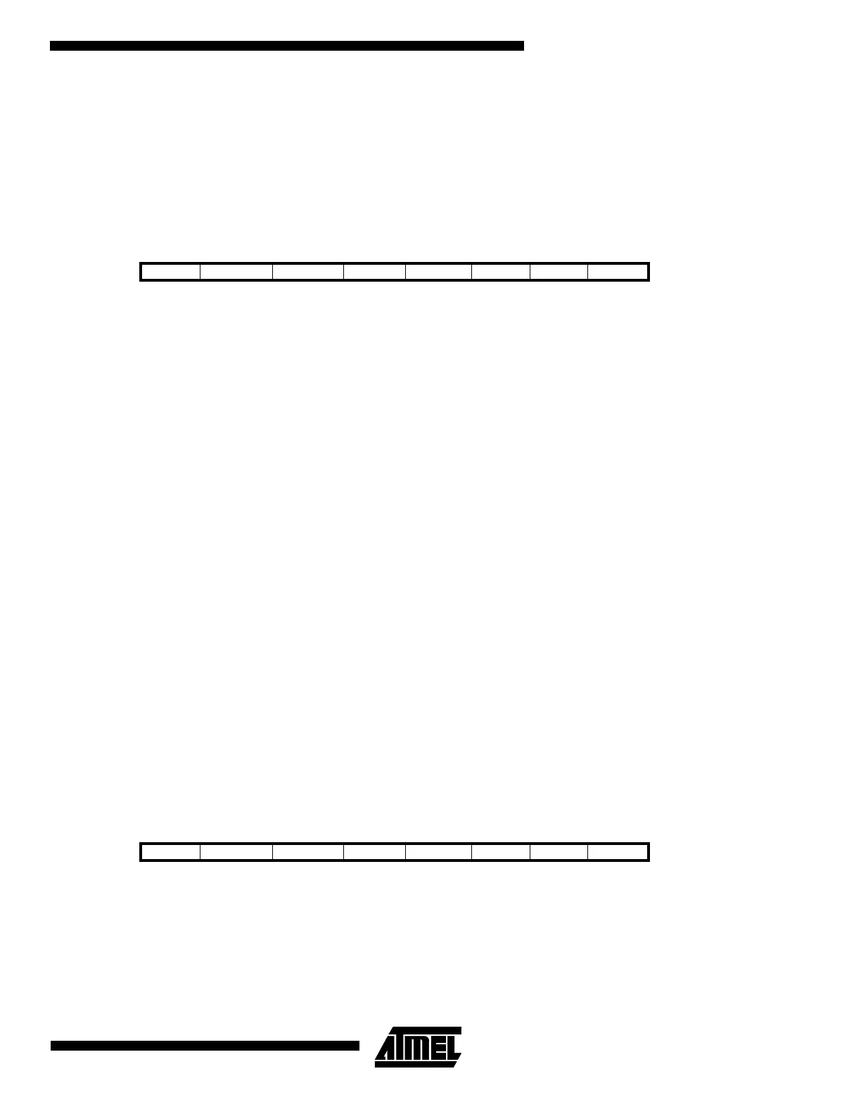
Bit 7 6 5 4 3 2 1 0
$39 ($59) TOIE1 OCIE1A OCIE1B - TICIE1 - TOIE0 - TIMSK
Read/Write R/W R/W R/W R R/W R R/W R
Initial value 0 0 0 0 0 0 0 0
Bit 7 6 5 4 3 2 1 0
$38 ($58) TOV1 OCF1A OCIFB - ICF1 - TOV0 - TIFR
Read/Write R/W R/W R/W R R/W R R/W R
Initial value 0 0 0 0 0 0 0 0
Question and Answer IconNeed help?

Do you have a question about the Atmel AT90S8515-8PI and is the answer not in the manual?

Atmel AT90S8515-8PI Specifications

General IconGeneral
Flash Memory8 KB
SRAM512 Bytes
EEPROM512 Bytes
Clock Speed8 MHz
I/O Pins32
USART1
Operating Temperature-40°C to +85°C
ManufacturerAtmel
ModelAT90S8515-8PI
ArchitectureAVR 8-bit
Communication InterfacesUSART
Package40-pin PDIP

Summary

Features

Specifications

Detailed technical specifications including power consumption, I/O, operating voltages, and speed grades.

Block Diagram

AT90S4414 vs AT90S8515 Comparison

Pin Descriptions

Port Pin Details (A, B, C, D)

Detailed description of each port's functionality, registers, and alternate functions.

Special Pin Functions

Explains the function of pins like RESET, XTAL, ICP, OC1B, and ALE.

Architectural Overview

Register File, ALU, and Addressing

Overview of the 32 working registers, ALU, and indirect addressing modes.

Memory Space Mapping

Details on I/O memory space for peripherals and data space mapping.

Memory Maps

General Purpose Register File

X, Y, and Z Registers for Addressing

Details on the X, Y, and Z registers used for indirect addressing.

Core Components and Memory

ALU Functionality

Description of the Arithmetic Logic Unit's role and operations.

Flash and SRAM Organization

Details on In-System Programmable Flash and SRAM organization.

Data Memory Addressing Modes

Register Direct Addressing

Explains how registers are accessed directly in instructions.

Data Memory Addressing Modes

Register Direct and I/O Direct

Covers direct register access and I/O register addressing.

Data Memory Addressing Modes

Data Direct and Indirect with Displacement

Explains direct data addressing and indirect addressing with displacement.

Data Memory Addressing Modes

Data Indirect Modes

Details indirect addressing, pre-decrement, and post-increment modes.

Data Memory Addressing Modes

Post-Increment and LPM Addressing

Covers indirect addressing with post-increment and LPM instruction.

Program Addressing Modes

Indirect and Relative Addressing

Explains indirect (IJMP, ICALL) and relative (RJMP, RCALL) program addressing.

EEPROM and Timing

EEPROM Data Memory

Details the EEPROM memory characteristics and organization.

Memory Access and Instruction Timing

Explains timing concepts for instruction execution and memory access.

I/O Memory

I/O Space Definition

Table listing I/O addresses, names, and functions for the MCU.

I/O Memory

SREG Status Register

Details the AVR Status Register (SREG) bits and their functions.

I/O Memory

Stack Pointer (SP)

Description of the 16-bit stack pointer and its usage.

Reset and Interrupt Handling

Interrupt Sources and Priority

Overview of interrupt sources, vectors, and priority levels.

Reset Sources

Power-On, External, and Watchdog Resets

Explains the three sources of MCU reset: Power-On, External, and Watchdog.

Reset Sources

Power-On Reset Behavior

Details the behavior and timing of the Power-on Reset circuit.

Reset Sources

External and Watchdog Reset

Explains external reset conditions and watchdog timer reset function.

Interrupt Handling

Interrupt Mask and Flag Registers

Describes GIMSK and GIFR for managing interrupt requests.

Interrupt Handling

Timer/Counter Interrupt Control

Details TIMSK for interrupt enables and TIFR for interrupt flags.

Interrupt Handling

External Interrupts and Response Time

Covers external interrupt configuration and interrupt response timing.

MCU Control Register (MCUCR)

MCUCR Bit Definitions

Explains bits for SRAM enable, sleep modes, and interrupt sense control.

MCU Control Register (MCUCR)

Sleep Modes (Idle and Power Down)

Describes the Idle and Power Down sleep modes and their wake-up sources.

Timer/Counters

General Timer/Counter Features

Overview of the 8-bit and 16-bit Timer/Counters.

Timer/Counters

Prescaler and Timer/Counter0

Details the prescaler selection and 8-bit Timer/Counter0.

Timer/Counters

TCCR0 Control Register

Explains the TCCR0 register bits for Timer/Counter0 clock select.

Timer/Counter1

TCNT1 Register

Describes the TCNT1H and TCNT1L registers for Timer/Counter1 value.

Timer/Counter1

TCCR1A Control Register

Details TCCR1A bits for compare output mode and PWM selection.

Timer/Counter1

TCCR1B Control Register

Explains TCCR1B bits for input capture and clock select.

Timer/Counter1

TCNT1 Register

Describes the TCNT1H and TCNT1L registers for Timer/Counter1 value.

Timer/Counter1

Output Compare Registers (OCR1A/B)

Details OCR1AH/AL and OCR1BH/BL for compare match functionality.

Timer/Counter1

Input Capture Register (ICR1) and PWM Mode

Covers ICR1 register and Timer/Counter1 PWM mode operation.

Watchdog Timer

WDTCR Control Register

Details WDTCR bits for enabling, disabling, and prescaling the watchdog.

EEPROM Read/Write Access

EEAR Address Registers

Describes EEARH and EEARL for specifying EEPROM addresses.

EEPROM Read/Write Access

EEDR and EECR Registers

Details EEDR for data transfer and EECR for write enable control.

Serial Peripheral Interface (SPI)

SPI Features

Lists key features of the SPI interface like full-duplex and master/slave operation.

Serial Peripheral Interface (SPI)

SS Pin Functionality

Explains the Slave Select (SS) pin behavior in master and slave modes.

Serial Peripheral Interface (SPI)

SPCR Control Register

Details SPCR bits for SPI enable, interrupt, data order, and mode select.

Serial Peripheral Interface (SPI)

SPSR and SPDR Registers

Describes SPSR for status flags and SPDR for data transfer.

UART

Data Transmission

Details the UART transmitter process and block diagram.

UART

Data Reception

Explains the UART receiver operation and block diagram.

UART

UART Control Register (UCR)

Describes UCR bits for receiver/transmitter enable and character format.

UART

USR Status Register

Details USR bits for receive/transmit complete and error flags.

UART

Baud Rate Generator

Explains the baud rate generator equation and UBRR settings.

UART

UBRR Register

Describes the UBRR register for setting the UART baud rate.

Analog Comparator

ACSR Control Register

Details ACSR bits for disabling, output, and interrupt control.

Interface to External SRAM

SRAM Interface Components

Lists components like Port A, Port C, ALE, RD, WR for SRAM interface.

I/O Ports

Port A Description

Covers Port A registers, I/O functions, and alternate functions.

I/O Ports

Port B Description

Details Port B registers, I/O functions, and alternate functions.

I/O Ports

Port B General I/O and Alternate Functions

Explains Port B digital I/O and its alternate pin configurations.

I/O Ports

Port C Description

Covers Port C registers, I/O functions, and alternate functions.

I/O Ports

Port D Description

Details Port D registers, I/O functions, and alternate functions.

Memory Programming

Lock Bits and Fuse Bits

Details lock bit protection modes and fuse bit configurations (SPIEN, FSTRT).

Signature Bytes

Information on device signature bytes for identification.

Memory Programming

Parallel Programming Overview

Describes parallel programming and signal name mapping.

Memory Programming

Enter Parallel Programming Mode

Step-by-step algorithm to enter parallel programming mode.

Memory Programming

Chip Erase and Flash Programming

Explains chip erase procedure and algorithm for programming Flash memory.

Memory Programming

Reading Flash/EEPROM and Programming Fuse Bits

Algorithms for reading Flash/EEPROM and programming Fuse bits.

Memory Programming

Lock Bits, Fuse/Lock Bits and Signature Bytes

Procedures for programming/reading lock bits, fuse bits, and signature bytes.

Parallel Programming Characteristics

Programming Timing

Details timing parameters for parallel programming operations.

Serial Downloading

SPI Serial Programming

Describes programming via SPI bus while RESET is low.

Serial Downloading

Serial Programming Algorithm and Data Polling

Algorithm for serial programming and data polling for EEPROM.

Serial Downloading

Data Polling Flash

Explains data polling for Flash programming to determine readiness.

Serial Programming Characteristics

Serial Programming Timing

Details timing parameters for serial programming operations.

Electrical Characteristics

Absolute Maximum Ratings

Lists the absolute maximum ratings for device operation.

DC Characteristics

Input/Output Voltage and Current

Details input/output voltage levels, leakage, and current specifications.

Power Supply and Analog Comparator Specs

Covers power supply current and analog comparator characteristics.

External Clock and RAM Timing

External Clock Drive Timing

Shows waveforms and parameters for external clock signals.

External SRAM Timing

Details timing for accessing external SRAM.

External Data Memory Timing

No Wait State Timing

Characteristics for external data memory access without wait states.

External Data Memory Timing

1 Cycle Wait State Timing

Characteristics for external data memory access with one wait state.

Typical Characteristics

Supply Current Characteristics

Graphs showing supply current in active, idle, and power-down modes.

Typical Characteristics

Analog Comparator and Watchdog Characteristics

Characteristics for analog comparator and watchdog oscillator frequency.

Typical Characteristics

I/O Port Characteristics

Graphs for pull-up resistor current, sink, source, and input hysteresis.

Register Summary

I/O Register Map

A comprehensive summary table of all I/O registers, their bits, and page references.

Instruction Set Summary

Arithmetic and Logic Instructions

Lists arithmetic and logic instructions, their operands, and flags.

Branch Instructions

Summarizes branch instructions, conditions, and jump targets.

Instruction Set Summary

Data Transfer and Bit Instructions

Lists data transfer, bit manipulation, and flag control instructions.

Ordering Information

Device Ordering Codes

Details ordering codes based on speed, power supply, package, and temperature.

Packaging Information

Package Types (TQFP, PLCC, PDIP)

Provides dimensions and details for TQFP, PLCC, and PDIP packages.

Related product manuals