AT90S4414/8515
33
Note: X = A or B
In PWM mode, these bits have a different function. Refer to Table 13 for a detailed description.
• Bits 3..2 - Res: Reserved bits
These bits are reserved bits in the AT90S4414/8515 and always read zero.
•
Bits 1..0 - PWM11, PWM10: Pulse Width Modulator Select Bits 1 and 0
These bits select PWM operation of Timer/Counter1 as specified in Table 10. This mode is described on page 36.
Timer/Counter1 Control Register B - TCCR1B
•
Bit 7 - ICNC1: Input Capture1 Noise Canceler (4 CKs)
When the ICNC1 bit is cleared (zero), the input capture trigger noise canceler function is disabled. The input capture is
triggered at the first rising/falling edge sampled on the ICP - input capture pin - as specified. When the ICNC1 bit is set
(one), four successive samples are measures on the ICP - input capture pin, and all samples must be high/low according to
the input capture trigger specification in the ICES1 bit. The actual sampling frequency is XTAL clock frequency.
•
Bit 6 - ICES1: Input Capture1 Edge Select
While the ICES1 bit is cleared (zero), the Timer/Counter1 contents are transferred to the Input Capture Register - ICR1 - on
the falling edge of the input capture pin - ICP. While the ICES1 bit is set (one), the Timer/Counter1 contents are transferred
to the Input Capture Register - ICR1 - on the rising edge of the input capture pin - ICP.
•
Bits 5, 4 - Res: Reserved bits
These bits are reserved bits in the AT90S4414/8515 and always read zero.
Table 9. Compare 1 Mode Select
COM1X1 COM1X0 Description
0 0 Timer/Counter1 disconnected from output pin OC1X
0 1 Toggle the OC1X output line.
1 0 Clear the OC1X output line (to zero).
1 1 Set the OC1X output line (to one).
Table 10. PWM Mode Select
PWM11 PWM10 Description
0 0 PWM operation of Timer/Counter1 is disabled
0 1 Timer/Counter1 is an 8-bit PWM
1 0 Timer/Counter1 is a 9-bit PWM
1 1 Timer/Counter1 is a 10-bit PWM
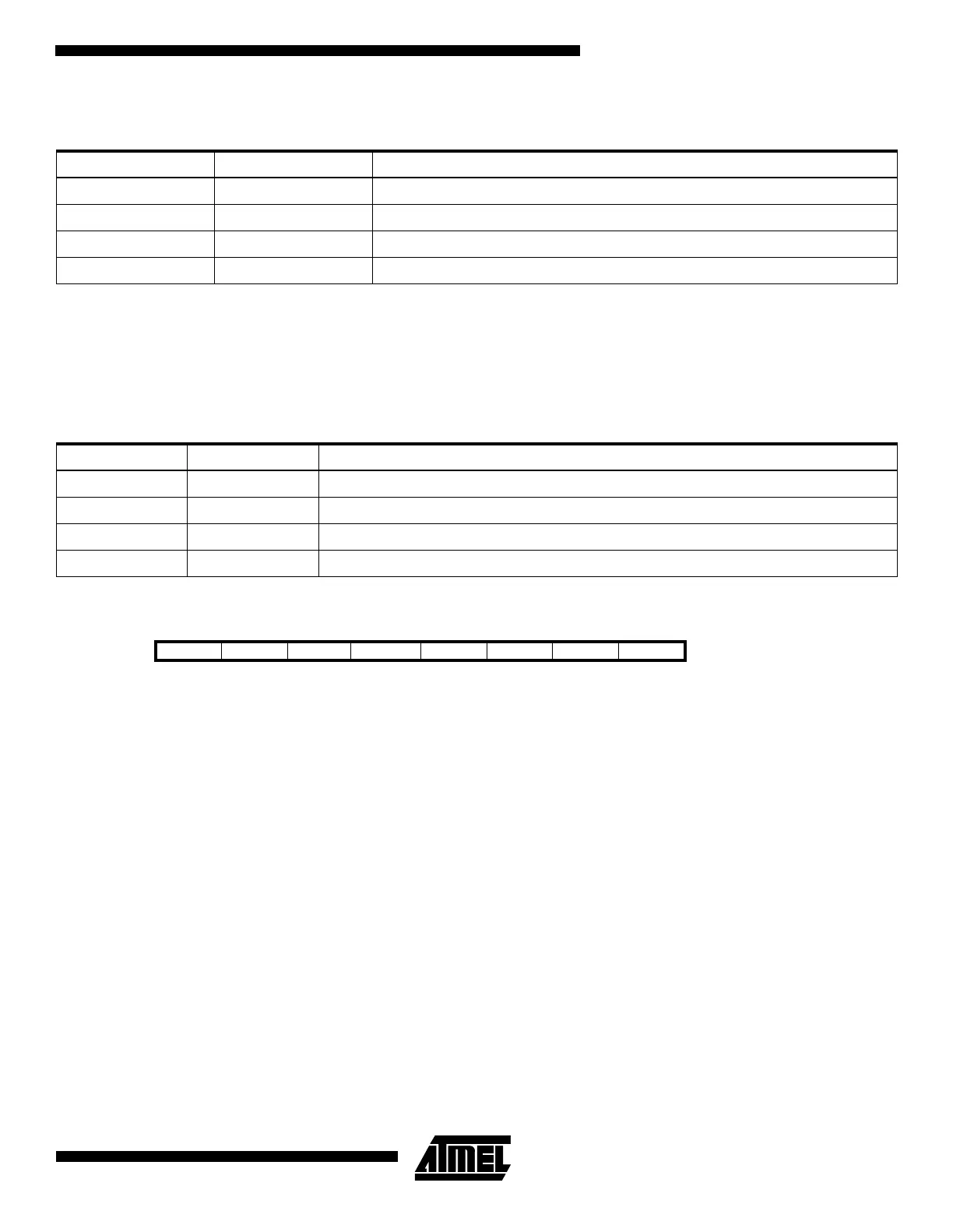
Bit 7 6 5 4 3 2 1 0
$2E ($4E) ICNC1 ICES1 - - CTC1 CS12 CS11 CS10 TCCR1B
Read/Write R/W R/W R R R/W R/W R/W R/W
Initial value 0 0 0 0 0 0 0 0

 Loading...


