AT90S4414/8515
64
Port D Data Register - PORTD
Port D Data Direction Register - DDRD
Port D Input Pins Address - PIND
The Port D Input Pins address - PIND - is not a register, and this address enables access to the physical value on each
Port D pin. When reading PORTD, the Port D Data Latch is read, and when reading PIND, the logical values present on the
pins are read.
PortD as General Digital I/O
PDn, General I/O pin: The DDDn bit in the DDRD register selects the direction of this pin. If DDDn is set (one), PDn is con-
figured as an output pin. If DDDn is cleared (zero), PDn is configured as an input pin. If PDn is set (one) when configured
as an input pin the MOS pull up resistor is activated. To switch the pull up resistor off the PDn has to be cleared (zero) or
the pin has to be configured as an output pin. The Port D pins are tri-stated when a reset condition becomes active, even if
the clock is not active.
n: 7,6…0, pin number.
Alternate Functions Of Port D
•
RD - Port D, Bit 7
RD is the external data memory read control strobe. See “Interface to External SRAM” on page 53 for detailed information.
•
WR - Port D, Bit 6
WR is the external data memory write control strobe. See “Interface to External SRAM” on page 53 for detailed information.
•
OC1A- Port D, Bit 5
OC1A, Output compare match output: The PD5 pin can serve as an external output when the Timer/Counter1 compare
matches. The PD5 pin has to be configured as an output (DDD5 set (one)) to serve this function. See the Timer/Counter1
description for further details, and how to enable the output. The OC1A pin is also the output pin for the PWM mode timer
function.
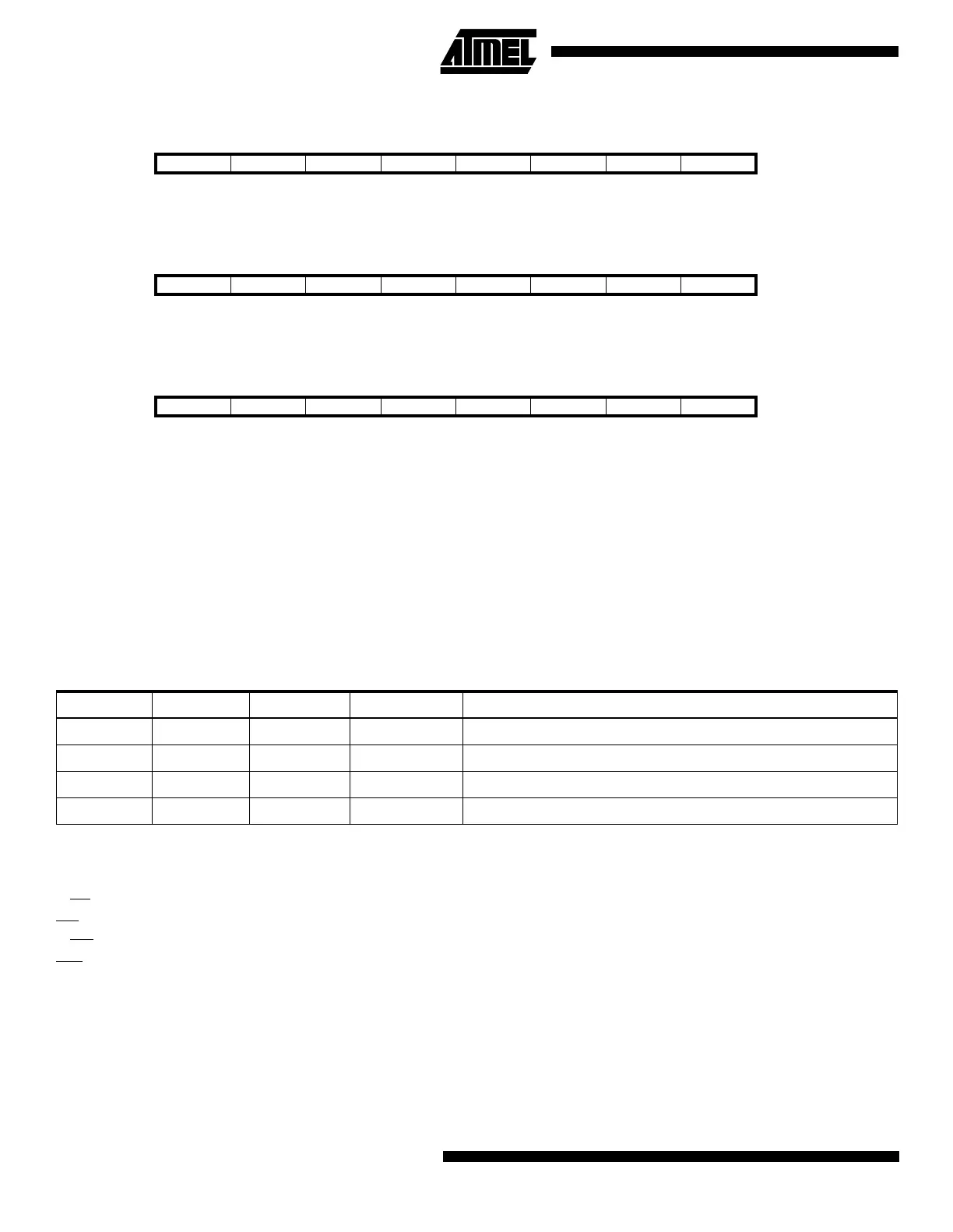
Bit 76543210
$12 ($32) PORTD7 PORTD6 PORTD5 PORTD4 PORTD3 PORTD2 PORTD1 PORTD0 PORTD
Read/Write R/W R/W R/W R/W R/W R/W R/W R/W
Initial value 0 0 0 0 0 0 0 0
Bit 76543210
$11 ($31) DDD7 DDD6 DDD5 DDD4 DDD3 DDD2 DDD1 DDD0 DDRD
Read/Write R/W R/W R/W R/W R/W R/W R/W R/W
Initial value 0 0 0 0 0 0 0 0
Bit 76543210
$10 ($30) PIND7 PIND6 PIND5 PIND4 PIND3 PIND2 PIND1 PIND0 PIND
Read/Write RRRRRRRR
Initial value Hi-Z Hi-Z Hi-Z Hi-Z Hi-Z Hi-Z Hi-Z Hi-Z
Table 25. DDDn Bits on Port D Pins
DDDn PORTDn I/O Pull up Comment
0 0 Input No Tri-state (Hi-Z)
0 1 Input Yes PDn will source current if ext. pulled low.
1 0 Output No Push-pull Zero Output
1 1 Output No Push-pull One Output

 Loading...


