AT90S4414/8515
63
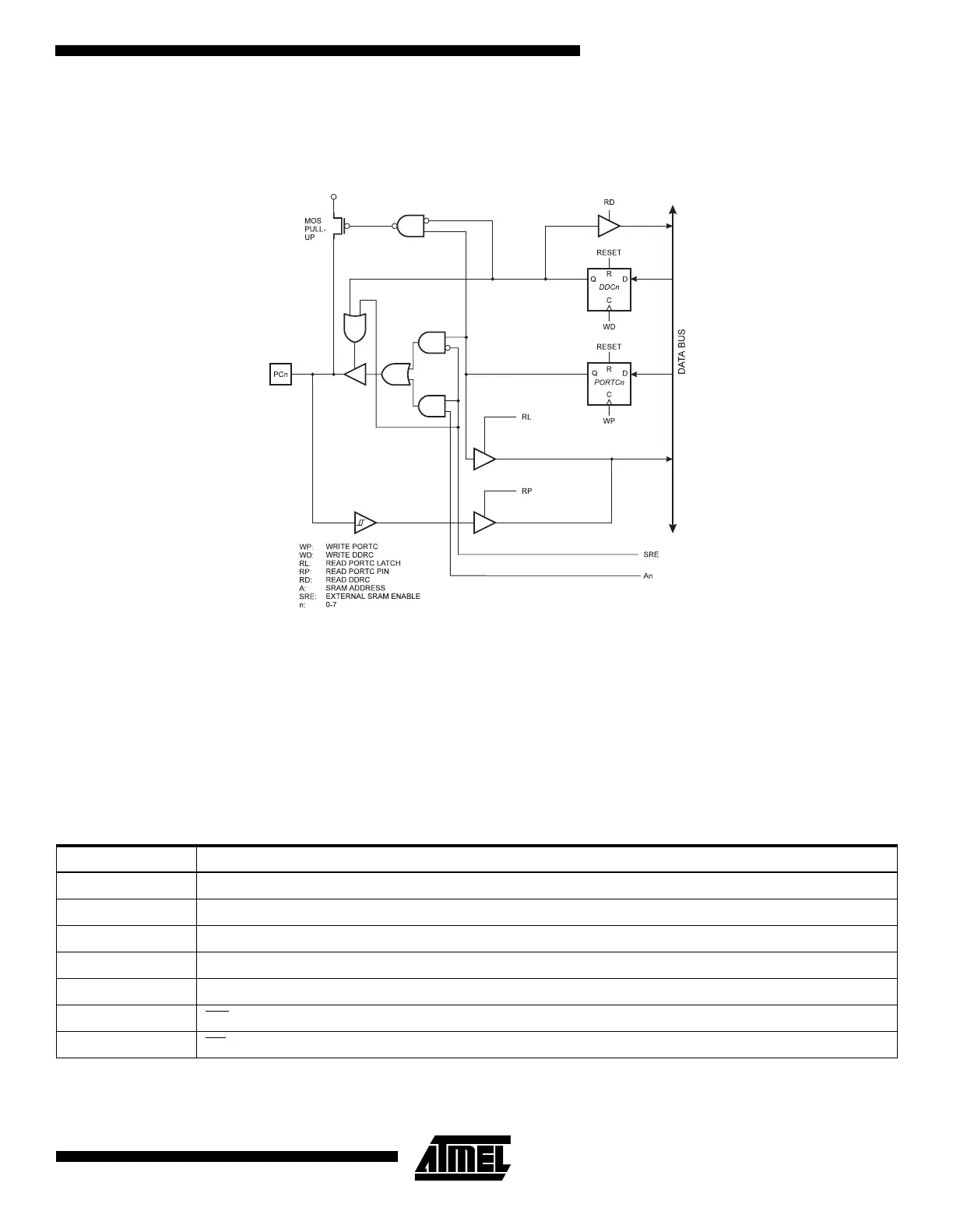
Port C Schematics
Note that all port pins are synchronized. The synchronization latch is however, not shown in the figure.
Figure 52. Port C Schematic Diagram (Pins PC0 - PC7)
Port D
Port D is an 8 bit bi-directional I/O port with internal pull-up resistors.
Three I/O memory address locations are allocated for the Port D, one each for the Data Register - PORTD, $12($32), Data
Direction Register - DDRD, $11($31) and the Port D Input Pins - PIND, $10($30). The Port D Input Pins address is read
only, while the Data Register and the Data Direction Register are read/write.
The Port D output buffers can sink 20 mA. As inputs, Port D pins that are externally pulled low will source current if the pull-
up resistors are activated.
Some Port D pins have alternate functions as shown in the following table:
When the pins are used for the alternate function the DDRD and PORTD register has to be set according to the alternate
function description.
Table 24. Port D Pins Alternate Functions
Port Pin Alternate Function
PD0 RXD (UART Input line)
PD1 TXD (UART Output line)
PD2 INT0 (External interrupt 0 input)
PD3 INT1 (External interrupt 1 input)
PD5 OC1A (Timer/Counter1 Output compareA match output)
PD6 WR
(Write strobe to external memory)
PD7 RD
(Read strobe to external memory)

 Loading...


